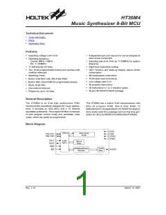
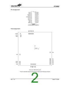
HT36M4
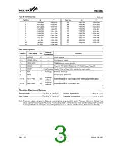
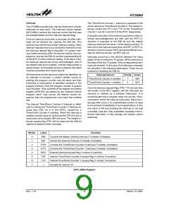
Pad Coordinates
Unit: mm
Pad No.
X
Y
Pad No.
X
Y
1
2
1261.050
1135.900
12
13
14
15
16
17
18
19
20
21
1146.750
1146.750
1146.750
1146.750
1146.750
1146.750
-153.300
-253.300
-363.900
-463.900
-1108.950
-1076.600
-1076.600
-1146.750
-1146.750
-1146.750
-1146.750
-292.374
-187.326
-85.550
-1250.000
-1139.400
-1039.400
-928.800
-828.800
-286.200
1256.550
1256.550
1256.550
1256.550
3
1030.900
-460.600
-1044.234
-1147.786
-1260.200
-1256.550
-1256.550
-1256.550
-1256.550
4
5
6
7
8
9
10
11
25.050
Pad Description
Internal
Connection
Pad No.
Pad Name
I/O
Function
1
AUDIO
VDDA, VSSA
VDD, VSS
OSC2
O
¾
¾
O
I
Audio output
DAC power supply
Digital power supply, ground
OUT or 1/4 system frequency in R mode (fOSC2=fOSC/8)
¾
¾
¾
¾
2, 3
7, 4
5
X
6
OSC1
X¢tal/Resistor XIN for X¢tal or ROSC in for resistor by mask option
8
INT
I
Pull-High
External interrupt
9
RES
I
Reset input, active low
¾
Pull-High
or None
17~10
21~18
PA7~PA0
PB0~PB3
I/O
I/O
Bidirectional 8-bit Input/Output port, wake-up by mask option
Bidirectional 8-bit input/output port
Pull-High
or None
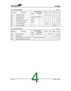
Absolute Maximum Ratings
Supply Voltage ..........................VSS-0.3V to VSS+5.5V
Input Voltage .............................VSS-0.3V to VDD+0.3V
Storage Temperature ...........................-50°C to 125°C
Operating Temperature ..........................-25°C to 70°C
Note: These are stress ratings only. Stresses exceeding the range specified under ²Absolute Maximum Ratings² may
cause substantial damage to the device. Functional operation of this device at other conditions beyond those listed
in the specification is not implied and prolonged exposure to extreme conditions may affect device reliability.
Rev. 1.10
3
March 14, 2007

 HOLTEK [ HOLTEK SEMICONDUCTOR INC ]