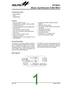
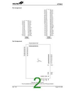
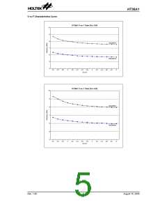
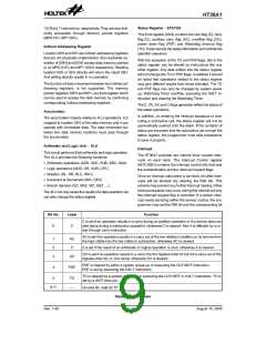
HT36A1
Pad Coordinates
Unit: mm
Pad No.
X
Y
Pad No.
X
Y
1
2
1271.550
1160.950
1060.950
950.350
18
19
20
21
22
23
24
25
26
27
28
29
30
31
32
33
959.450
959.450
959.450
959.450
959.450
959.450
959.450
959.450
-46.550
-157.150
-257.150
-367.750
-467.750
-578.350
-678.350
-788.950
-959.800
-959.800
-959.800
-959.800
-959.800
-959.800
-959.800
-959.800
279.300
392.300
504.750
649.850
770.100
944.700
919.650
919.650
919.650
-152.100
-41.500
58.500
3
4
169.100
269.100
379.700
479.700
590.300
1386.150
1386.150
1386.150
1386.150
1386.150
1386.150
1386.150
1386.150
5
850.350
6
739.750
7
639.750
8
529.150
9
-1352.350
-1352.350
-1352.450
-1352.300
-1352.400
-1345.670
-1133.274
-1014.076
-336.224
10
11
12
13
14
15
16
17
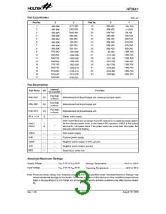
Pad Description
Internal
Connection
Pad Name I/O
Function
Pull-High
or None
PA0~PA7
PB0~PB7
I/O
I/O
Bidirectional 8-bit Input/Output port, wake-up by mask option
Bidirectional 8-bit Input/Output port
Pull-High
or None
Pull-High
or None
PC0~PC7
RCH, LCH
I/O
O
Bidirectional 8-bit Input/Output port
Stereo audio output
¾
OSC1 and OSC2 are connected to an RC network or a crystal (by mask option)
for the internal system clock. In the case of RC operation, OSC2 is the output
terminal for 1/8 system clock. The system clock may come from the crystal, the
two pins cannot be floating.
OSC1
OSC2
I
¾
O
VDDA
VDD
DAC power supply
¾
¾
¾
¾
I
¾
¾
¾
¾
¾
Positive power supply
VSSA
VSS
Negative power supply of DAC, ground
Negative power supply, ground
Reset input, active low
RES
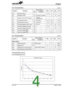
Absolute Maximum Ratings
Supply Voltage ..........................VSS-0.3V to VSS+5.5V
Input Voltage .............................VSS-0.3V to VDD+0.3V
Storage Temperature ...........................-50°C to 125°C
Operating Temperature ..........................-25°C to 70°C
Note: These are stress ratings only. Stresses exceeding the range specified under ²Absolute Maximum Ratings² may
cause substantial damage to the device. Functional operation of this device at other conditions beyond those
listed in the specification is not implied and prolonged exposure to extreme conditions may affect device reliabil-
ity.
Rev. 1.00
3
August 15, 2005

 HOLTEK [ HOLTEK SEMICONDUCTOR INC ]