ꢃꢅ-bit �RM Coꢁtex™-Mꢃ MCU
HTꢃꢅF1ꢅ51/51B/5ꢅ/5ꢃ
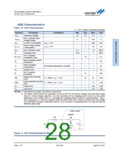
The worst case occurs when the extremities of the input range (0V and VREF) are sampled consecutively.
In this situation a sampling error below ¼ LSB is ensured by using the following equation:
1.5
RS <
− RI
fADCCI ln(2N +2
)
where fADC is the ADC clock frequency and N is the ADC resolution (N = 12 in this case). A safe
margin should be considered due to the pin/pad parasitic capacitances, which are not accounted for
in this simple model.
If, in a system where this A/D Converter is used, there are no rail-to-rail input voltage variations between
consecutive sampling phases, Rs may be larger than the value indicated by the equation above.
Operation Amplifier/Comparator Characteristics
Table 16. OPA/CMP Characteristics
T� = ꢅ5°C, unless otherwise specified.
Symbol
VDD�
Parameter
Conditions
Min
ꢅ.7
—
Typ
ꢃ.ꢃ
Max
ꢃ.6
—
Unit
V
Oꢀeꢁating Voꢂtage
Tyꢀicaꢂ Oꢀeꢁating Cuꢁꢁent
—
—
IOP�/CMP
ꢅꢃ0
u�
�ssign ꢁegisteꢁs OP�EN = 0
and EN_OP�OP = 0
IOP�/CMP_DN Poweꢁ Down Suꢀꢀꢂy Cuꢁꢁent
—
—
—
0.1
15
u�
VDD� = ꢃ.ꢃVꢄ
�nOF[5:0] = ‘100000’
-15
mV
VIOS
Inꢀut Offset Voꢂtage
VDD� = ꢃ.ꢃVꢄ �fteꢁ caꢂibꢁation
-1
—
—
—
1
0.04
—
mV
VIOS_DRIFT Inꢀut Offset Voꢂtage Dꢁift
T� = -40°C ~ +85°C
mV/°C
RINPUT
GV
Inꢀut Resistance
Voꢂtage Gain
—
—
—
10
M
W
60
100
1ꢄꢃ
1.ꢅ4
—
—
dB
MHz
V
RL=100kΩ
—
—
Ut
Unit-Gain Bandwidth
RL=100kΩ, CL=100ꢀF
—
—
VCM
VOV
Common Mode Voꢂtage Range VDD� = ꢃ.ꢃV
VSS�
VSS�+0.ꢃ
VDD� – 1.ꢅ
OP� Outꢀut Voꢂtage Wwing
VDD� = ꢃ.ꢃV
—
VDD� – 0.5 V/us
VDD� = ꢃ.ꢃV;
Inꢀut Oveꢁdꢁive = ±10mV
tRT
Comꢀaꢁatoꢁ Resꢀonse Time
—
—
1.6
1
—
—
us
VDD� = ꢃ.ꢃV; Outꢀut caꢀacitoꢁ
ꢂoad CL=100ꢀF
SR
Sꢂew Rate
V/us
NOTE: Guaꢁanteed by designꢄ not tested in ꢀꢁoduction.
GPTM Characteristics
Table 17. GPTM Characteristics
Symbol
fGPTM
Parameter
Conditions
Min
—
1
Typ
Max
7ꢅ
Unit
MHz
1/fGPTM
fGPTM
bits
Timeꢁ cꢂock souꢁce
—
—
—
—
—
—
—
—
tRES
Timeꢁ ꢁesoꢂution time
—
fEXT
Exteꢁnaꢂ signaꢂ fꢁequency on channeꢂ 1 ~ 4
Timeꢁ ꢁesoꢂution
—
—
1/ꢅ
16
RES
Rev. 1.10
ꢅ9 of ꢃ5
�ꢀꢁiꢂ 1ꢃꢄ ꢅ01ꢅ

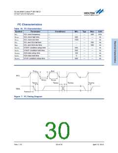
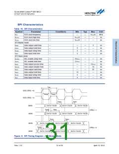
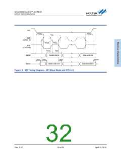
 HOLTEK [ HOLTEK SEMICONDUCTOR INC ]