ꢃꢅ-bit �RM Coꢁtex™-Mꢃ MCU
HTꢃꢅF1ꢅ51/51B/5ꢅ/5ꢃ
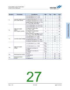
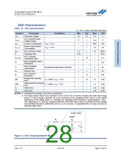
ADC Characteristics
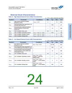
Table 15. ADC Characteristics
T� = ꢅ5°C, unless otherwise specified.
Symbol
Parameter
Conditions
Min
Typ
Max
Unit
VDD�
Oꢀeꢁating Voꢂtage
ꢅ.7
ꢃ.ꢃ
ꢃ.6
V
�/D Conveꢁteꢁ Inꢀut
voꢂtage Range
V�DCIN
I�DC
0
—
1
VDD�
TBD
10
V
Cuꢁꢁent Consumꢀtion
VDD� = ꢃ.ꢃV
VDD� = ꢃ.ꢃV
—
—
m�
u�
Poweꢁ Down cuꢁꢁent
Consumꢀtion
I�DC_DN
1
f�DC
fS
�/D Conveꢁteꢁ Cꢂock
Samꢀꢂing Rate
0.7
—
—
14
1
MHz
MHz
0.05
�/D Conveꢁteꢁ
Conveꢁsion Time
f�DCCONV
RI
—
—
14
—
—
1
t�DC
Inꢀut Samꢀꢂing Switch
Resistance
kΩ
Inꢀut Samꢀꢂing
Caꢀacitance
CI
tSU
N
No ꢀin/ꢀad caꢀacitance incꢂuded
—
—
—
—
—
1ꢅ
5
1
ꢀF
us
Staꢁtuꢀ Time
�/D Conveꢁteꢁ
Resoꢂution
—
bits
Integꢁaꢂ Non-ꢂineaꢁity
eꢁꢁoꢁ
INL
fS = 1MHzꢄ VDD� = ꢃ.ꢃV
fS = 1MHzꢄ VDD� = ꢃ.ꢃV
-—
—
±ꢅ
—
±5
±1
LSB
LSB
Diffeꢁentiaꢂ Non-ꢂineaꢁity
eꢁꢁoꢁ
DNL
EO
EG
Offset Eꢁꢁoꢁ
Gain Eꢁꢁoꢁ
—
—
—
—
±10
±10
LSB
LSB
NOTES: 1. Guaꢁanteed by designꢄ not tested in ꢀꢁoduction.
2. The figuꢁe beꢂow shows the equivaꢂent ciꢁcuit of the �/D Conveꢁteꢁ Samꢀꢂe-and-Hoꢂd inꢀut stage
wheꢁe CI is the stoꢁage caꢀacitoꢁꢄ RI is the ꢁesistance of the samꢀꢂing switch and RS is the outꢀut
imꢀedance of the signaꢂ souꢁce VS. Noꢁmaꢂꢂy the samꢀꢂing ꢀhase duꢁation is aꢀꢀꢁoximateꢂyꢄ 1.5/f�DC
.
The caꢀacitanceꢄ CIꢄ must be chaꢁged within this time fꢁame and it must be ensuꢁed that the voꢂtage
at its terminals becomes sufficiently close to VS foꢁ accuꢁacy. To guaꢁantee thisꢄ RS may not have an
aꢁbitꢁaꢁiꢂy ꢂaꢁge vaꢂue.
SAR ADC
sample
RS
CI
VS
RI
Figure 6. ADC Sampling Network Model
Rev. 1.10
ꢅ8 of ꢃ5
�ꢀꢁiꢂ 1ꢃꢄ ꢅ01ꢅ

 HOLTEK [ HOLTEK SEMICONDUCTOR INC ]