19.5
Flash Memory Emulation by RAM
Erasing and programming flash memory takes time, which can make it difficult to tune parameters
and other data in real time. If necessary, real-time updates of flash memory can be emulated by
overlapping the small-block flash-memory area with part of the RAM (H'FC00 to H'FD7F). This
RAM reassignment is performed using bits 7 and 6 of the wait-state control register (WSCR).
After a flash memory area has been overlapped by RAM, the RAM area can be accessed from two
address areas: the overlapped flash memory area, and the original RAM area (H'FC00 to H'FD7F).
Table 19.11 indicates how to reassign RAM.
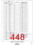
Wait-State Control Register (WSCR)*2
Bit
7
RAMS
0
6
RAM0
0
5
CKDBL
0
4
—
3
WMS1
1
2
WMS0
0
1
WC1
0
0
WC0
0
Initial value*1
Read/Write
0
R/W
R/W
R/W
R/W
R/W
R/W
R/W
R/W
Notes: *1 WSCR is initialized by a reset and in hardware standby mode. It is not initialized in
software standby mode.
*2For details of WSCR settings, see section 19.2.4, Wait-State Control Register (WSCR
Table 19.11 RAM Area Selection
Bit 7: RAMS
Bit 6: RAMO
RAM Area
ROM Area
0
0
1
0
1
None
—
H'FC80 to H'FCFF
H'FC80 to H'FD7F
H'FC00 to H'FC7F
H'0080 to H'00FF
H'0080 to H'017F
H'0000 to H'007F
1
415

 HITACHI [ HITACHI SEMICONDUCTOR ]