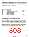
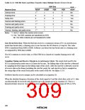
Table 12.12 SSR Bit States and Data Transfer when Multiple Receive Errors Occur
SSR Bits
RSR →
Receive Error
RDRF
1*1
0
ORER
FER
0
PER
RDR*2
Overrun error
1
0
0
1
1
0
1
0
0
1
0
1
1
1
No
Framing error
1
Yes
Yes
No
Parity error
0
0
Overrun and framing errors
Overrun and parity errors
Framing and parity errors
Overrun, framing, and parity errors
1*1
1*1
0
1
0
No
1
Yes
No
1*1
1
Notes: *1 Set to 1 before the overrun error occurs.
*2 Yes: The RSR contents are transferred to RDR.
No: The RSR contents are not transferred to RDR.
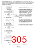
Line Break Detection: When the RxD pin receives a continuous stream of 0’s in asynchronous
mode (line-break state), a framing error occurs because the SCI detects a 0 stop bit. The value
H'00 is transferred from RSR to RDR. Software can detect the line-break state as a framing error
accompanied by H'00 data in RDR.
The SCI continues to receive data, so if the FER bit is cleared to 0 another framing error will
occur.
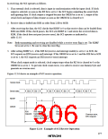
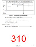
Sampling Timing and Receive Margin in Asynchronous Mode: The serial clock used by the
SCI in asynchronous mode runs at 16 times the bit rate. The falling edge of the start bit is detected
by sampling the RxD input on the falling edge of this clock. After the start bit is detected, each bit
of receive data in the frame (including the start bit, parity bit, and stop bit or bits) is sampled on
the rising edge of the serial clock pulse at the center of the bit. See figure 12.18.
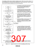
It follows that the receive margin can be calculated as in equation (1).
When the absolute frequency deviation of the clock signal is 0 and the clock duty cycle is 0.5, data
can theoretically be received with distortion up to the margin given by equation (2). This is a
theoretical limit, however. In practice, system designers should allow a margin of 20% to 30%.
280

 HITACHI [ HITACHI SEMICONDUCTOR ]