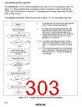
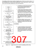
Transmitting and Receiving Serial Data Simultaneously: Follow the procedure in figure 12.17
for transmitting and receiving serial data simultaneously. If clock output mode is selected, output
of the serial clock begins simultaneously with serial transmission.
1. SCI initialization: the transmit data output function of
the TxD pin and receive data input function of the
1
2
Initialize
Start
RxD pin are selected, enabling simultaneous
transmitting and receiving.
2. SCI status check and transmit data write: read the
serial status register (SSR), check that the TDRE bit
is 1, then write transmit data in the transmit data
register (TDR) and clear TDRE to 0. Transition of the
TDRE bit from 0 to 1 can be reported by a TXI interrupt.
Read TDRE bit in SSR
No
TDRE = 1?
Yes
3. SCI status check and receive data read: read the
serial status register (SSR), check that the RDRF
bit is 1, then read receive data from the receive data
register (RDR) and clear RDRF to 0. Transition of
the RDRF bit from 0 to 1 can be reported by an RXI
interrupt.
3
Write transmit data
in TDR and clear TDRE
bit to 0 in SSR
4. Receive error handling: if a receive error occurs, read
the ORER bit in SSR then, after executing the
necessary error handling, clear ORER to 0. Neither
transmitting nor receiving can resume while ORER
remains set to 1.
Read ORER bit in SSR
ORER = 1?
Yes
4
No
Error handling
Read RDRF bit in SSR
5. To continue transmitting and receiving serial data:
No
RDRF = 1?
Yes
read RDR and clear RDRF to 0 before the MSB
(bit 7) of the current frame is received. Also read the
TDRE bit and check that it is set to 1, indicating that
it is safe to write; then write data in TDR and clear
TDRE to 0 before the MSB (bit 7) of the current frame
is transmitted.
Read receive data
from RDR and clear
RDRF bit to 0 in SSR
5
End of
transmitting and
receiving?
No
Yes
Clear TE and RE bits
to 0 in SCR
End
Note: In switching from transmitting or receiving to simultaneous transmitting and receiving, clear both
TE and RE to 0, then set TE and RE to 1 simultaneously using an MOV instruction. Do not use a
BEST instruction for this purpose.
Figure 12.17 Sample Flowchart for Serial Transmitting and Receiving
278

 HITACHI [ HITACHI SEMICONDUCTOR ]