12.3.3 Synchronous Mode
Overview
In synchronous mode, the SCI transmits and receives data in synchronization with clock pulses.
This mode is suitable for high-speed serial communication.
The SCI transmitter and receiver share the same clock but are otherwise independent, so full
duplex communication is possible. The transmitter and receiver are also double buffered, so
continuous transmitting or receiving is possible by reading or writing data while transmitting or
receiving is in progress.
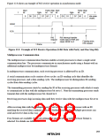
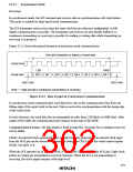
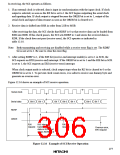
Figure 12.12 shows the general format in synchronous serial communication.
One unit (character or frame) of serial data
*
*
Serial clock
Serial data
LSB
Bit 0
MSB
Bit 7
Bit 1
Bit 2
Bit 3
Bit 4
Bit 5
Bit 6
Don’t care
Note: * High except in continuous transmitting or receiving
Don’t care
Figure 12.12 Data Format in Synchronous Communication
In synchronous serial communication, each data bit is sent on the communication line from one
falling edge of the serial clock to the next. Data is received in synchronization with the rising edge
of the serial clock.
In each character, the serial data bits are transmitted in order from LSB (first) to MSB (last). After
output of the MSB, the communication line remains in the state of the MSB.
Communication Format: The data length is fixed at eight bits. No parity bit or multiprocessor bit
can be added.
Clock: An internal clock generated by the on-chip baud rate generator or an external clock input
from the SCK pin can be selected by clearing or setting the CKE1 bit in the serial control register
(SCR). See table 12.8.
When the SCI operates on an internal clock, it outputs the clock signal at the SCK pin. Eight clock
pulses are output per transmitted or received character. When the SCI is not transmitting or
receiving, the clock signal remains at the high level.
273

 HITACHI [ HITACHI SEMICONDUCTOR ]