Transmitting Multiprocessor Serial Data: See figures 12.5 and 12.6.
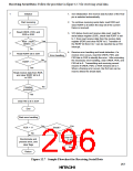
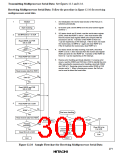
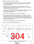
Receiving Multiprocessor Serial Data: Follow the procedure in figure 12.10 for receiving
multiprocessor serial data.
1
2
Initialize
1. SCI initialization: the receive data function of the RxD pin is
selected automatically.
2. ID receive cycle: Set the MPIE bit in the serial control register
(SCR) to 1.
Start receiving
3. SCI status check and ID check: read the serial status register
(SSR), check that RDRF is set to 1, then read receive data
from the receive data register (RDR) and compare with the
processor’s own ID. Transition of the RDRF bit from 0 to
1 can be reported by an RXI interrupt. If the ID does not match
the receive data, set MPIE to 1 again and clear RDRF to 0.
If the ID matches the receive data, clear RDRF to 0.
Set MPIE bit to 1 in SCR
Read ORER and FER
bits in SSR
FER
ORER = 1?
Yes
No
4. SCI status check and data receiving: read SSR, check that
RDRF is set to 1, then read data from the receive data register
(RDR) and write 0 in the RDRF bit. Transition of the RDRF bit
from 0 to 1 can be reported by an RXI interrupt.
No
3
Read RDRF bit in SSR
5. Receive error handling and break detection: if a receive error
occurs, read the ORER and FER bits in SSR to identify the error.
After executing the necessary error handling, clear both ORER
and FER to 0. Receiving cannot resume while ORER or FER
remains set to 1. When a framing error occurs, the RxD pin
can be read to detect the break state.
RDRF = 1?
Yes
Read receive data from RDR
No
Own ID?
Yes
Read ORER and FER
bits in SSR
FER +
Yes
ORER = 1?
No
4
Read RDRF bit in SSR
No
RDRF = 1?
Yes
Start error handling
5
Read receive data from RDR
Yes
Yes
FER = 1?
No
Break?
No
Error handling
No
Finished
receiving?
Clear RE bit to
0 in SCR
Discriminate and
process error, and
clear flags
Yes
Clear RE to 0 in SCR
End
Return
End
Figure 12.10 Sample Flowchart for Receiving Multiprocessor Serial Data
271

 HITACHI [ HITACHI SEMICONDUCTOR ]