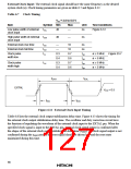
Table 6.8 External Clock Output Stabilization Delay Time
Conditions: VCC = 3.0 to 5.5 V, AVCC = 2.7 to 5.5 V, VSS = AVSS = 0 V
Item
Symbol
tDEXT
Min
Max
Unit
Notes
External clock output stabilization
delay time
*
500
—
µs
Figure 6.13
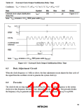
Note: * tDEXT includes a 10 tcyc RES pulse width (tRESW).
VCC
3.0 V
VIH
STBY
EXTAL
ø (internal and
external)
RES
tDEXT
*
Note: * tDEXT includes a 10 tcyc RES pulse width (tRESW).
Figure 6.13 External Clock Output Stabilization Delay Time
6.3
Duty Adjustment Circuit
When the clock frequency is 5 MHz or above, the duty adjustment circuit adjusts the duty cycle of
the signal from the oscillator circuit to generate the system clock (ø).
6.4
Prescaler
The clock for the on-chip supporting modules (øP) has either the same frequency as the system
clock (ø) or this frequency divided by two, depending on the CKDBL bit. The prescaler divides
the frequency of øP to generate internal clock signals with frequencies from øP/2 to øP/4096.
99

 HITACHI [ HITACHI SEMICONDUCTOR ]