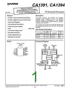
CA1391, CA1394
Application Information
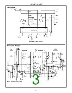
Circuit Operation (See Schematic Diagram)
Q
and Q so that there is no net output current at Terminal 5
21
20
for balanced conditions. When a phase offset occurs, current
flows either in or out of Terminal 5. In circuit applications, this
terminal is connected to Terminal 7 through an external low
pass filter, thereby controlling the oscillator.
The CA1391 and CA1394 contain the oscillator, phase
detector, and predriver sections necessary for the television
horizontal oscillator and AFC loop.
The oscillator is an RC type with Terminal 7 used to control the
Shunt regulation for the circuit is obtained by using a V
BE
BE
timing. If it is assumed that Q is initially off, then an external
7
and zener multiplier. Resistors R and R multiply the V
13 14
capacitor connected from Terminal 7 to ground charges through
an external resistance connected between Terminals 6 and 7. As
soon as the voltage at Terminal 7 exceeds the potential set at the
of Q , and the ratio of R and R multiplies the voltage of
11 15 16
the zener diode Z .
1
base of Q by resistors R and R , Q turns on, and Q sup-
8
11 12
7
6
plies base current to Q and Q . Transistor Q discharges the
o
5
10
5
T
= 25 C
A
5.0
4.5
4.0
3.5
3.0
2.5
2.0
capacitor through R until the base bias of Q falls below that of
4
7
FREE RUNNING FREQUENCY = 15734Hz
Q at which time, Q turns off, and the cycle repeats.
8
7
The sawtooth generated at the base of Q appears across R
4
3
and turns off Q whenever the sawtooth voltage rises to a value
3
that exceeds the bias set at Terminal 8. By adjusting the poten-
tial at Terminal 8, the duty cycle at the pre-drive output (Termi-
nal 1) may be changed. The phase detector is isolated from the
remainder of the circuit by R , Z , Q and Q . The phase
31 15 16
2
detector consists of the comparator Q and Q , and the
22 23
gated current source Q . Negative going sync pulses at Ter-
18
minal 3 turn off Q , and the current division between Q and
17 22
is then determined by the phase relationship of the sync
Q
23
and the sawtooth waveform at Terminal 4, which is derived from
the horizontal flyback pulse. If there is no phase difference
between the sync and sawtooth, equal currents flow in the col-
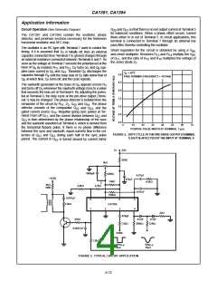
0
10
20
30
40
50
60
70
POSITIVE PULSE WIDTH AT TERMINAL 1 (µs)
FIGURE 2. DUTY CYCLE AT THE PRE-DRIVE OUTPUT (TERMINAL
1) AS IT IS AFFECTED BY THE INPUT AT TERMINAL 8
lectors of Q and Q during each half of the sync pulse
period. The current in Q is turned around by current mirror
22
22 23
V+
24V
620Ω
3kΩ
6800pF
120kΩ
0.47µF
0.01µF
+150V
470µF
14kΩ
8.2kΩ
2
4kΩ
10W
2.4kΩ
2.7kΩ
150kΩ
0.001µF
1.5kΩ
8
1
7
2
6
3
5
4
CA1394
22Ω
470pF
270Ω
0.1µF
0.1µF
3.9kΩ
7.5kΩ
390kΩ
0.0027µF
SYNC
1.2kΩ
20V
5µs
60V
P-P
10µs
P-P
FIGURE 3. TYPICAL CIRCUIT APPLICATION
8-12

 HARRIS [ HARRIS CORPORATION ]