CA1391, CA1394
Absolute Maximum Ratings
Thermal Information
o
DC Supply Current . . . . . . . . . . . . . . . . . . . . . . . . . . . . . . . . . 40mA Thermal Resistance (Typical, Note 1)
θJA ( C/W)
DC Output Voltage . . . . . . . . . . . . . . . . . . . . . . . . . . . . . . . . . . . 40V
DC Output Current . . . . . . . . . . . . . . . . . . . . . . . . . . . . . . . . . 30mA
PDIP Package . . . . . . . . . . . . . . . . . . . . . . . . . . . . .
Maximum Junction Temperature (Plastic Package) . . . . . . . . 150 C
Maximum Storage Temperature Range . . . . . . . . . -65 C to 150 C
Maximum Lead Temperature (Soldering 10s) . . . . . . . . . . . . . 300 C
120
o
o
o
Sync Input Voltage . . . . . . . . . . . . . . . . . . . . . . . . . . . . . . . . . 5V
Sawtooth Input Voltage. . . . . . . . . . . . . . . . . . . . . . . . . . . . . . 5V
P-P
P-P
o
Operating Conditions
o
o
Temperature Range . . . . . . . . . . . . . . . . . . . . . . . . . . . 0 C to 85 C
CAUTION: Stresses above those listed in “Absolute Maximum Ratings” may cause permanent damage to the device. This is a stress only rating and operation
of the device at these or any other conditions above those indicated in the operational sections of this specification is not implied.
NOTE:
1. θ is measured with the component mounted on an evaluation PC board in free air.
JA
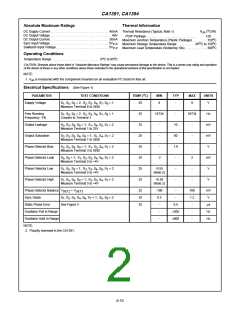
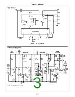
Electrical Specifications (See Figure 1)
o
PARAMETER
Supply Voltage
TEST CONDITIONS
S , S , S = 2; S , S , S , S , S = 1
TEMP. ( C)
MIN
TYP
MAX
UNITS
25
8
-
9
V
1
5
6
2
3
4
7
8
Measure Terminal 6 to GND
Free Running
Frequency -1%
S , S , S = 2; S , S , S , S , S = 1
Counter to Terminal 1
25
25
25
25
25
25
25
14734
-
10
60
1.9
-
16734
Hz
mV
mV
V
1
5
6
2
3
4
7
8
Output Leakage
S , S , S , S = 1; S , S , S , S = 2
-
-
-
-
2
3
6
8
1
4
5
7
Measure Terminal 1 to 25V
Output Saturation
Phase Detector Bias
Phase Detector Leak
Phase Detector Low
Phase Detector High
S , S , S , S , S = 1; S , S , S = 2
2
3
5
6
8
1
4
7
Measure Terminal 1 to GND
S , S , S , S = 1; S , S , S , S = 2
-
-
2
5
6
8
1
3
4
7
Measure Terminal 3 to GND
S , S = 1; S , S , S , S , S , S = 2
-2
2
-
mV
V
5
8
1
2
3
4
6
7
Measure Terminal 5 to +4V
S , S , S = 1; S , S , S , S , S = 2
-0.55
(Note 2)
-
1
5
8
2
3
4
6
7
Measure Terminal 5 to +4V
S , S , S , S = 1; S , S , S , S = 2
+0.55
-
-
V
1
5
6
8
2
3
4
7
Measure Terminal 5 to +4V
(Note 2)
Phase Detector Balance V
DET2
+ V
DET3
25
25
25
-100
-
100
mV
V
Sync Diode
S , S , S , S , S , S = 1; S , S = 2
0.3
-
1.2
1
2
3
4
6
7
5
8
Static Phase Error
Oscillator Pull In Range
Oscillator Hold In Range
NOTE:
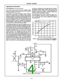
See Figure 3
-
-
-
0.5
±300
±900
-
-
-
µs
Hz
Hz
2. Polarity reversed in the CA1391.
8-10

 HARRIS [ HARRIS CORPORATION ]