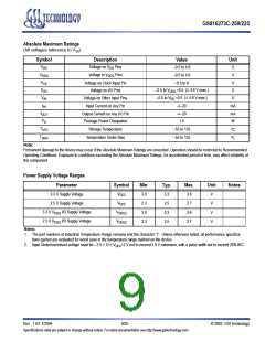
GS816273C-250/225
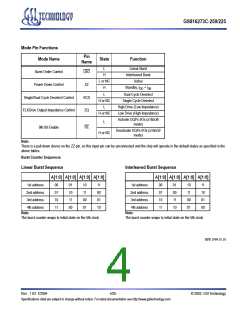
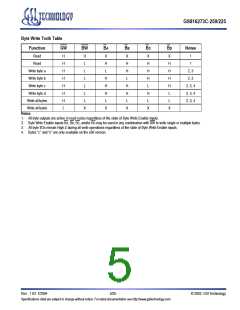
Mode Pin Functions
Mode Name
Pin
Name
State
Function
L
Linear Burst
Interleaved Burst
Active
Burst Order Control
Power Down Control
LBO
H
L or NC
ZZ
Standby, I = I
H
DD SB
L
Dual Cycle Deselect
Single Cycle Deselect
Single/Dual Cycle Deselect Control
FLXDrive Output Impedance Control
SCD
ZQ
H or NC
L
High Drive (Low Impedance)
Low Drive (High Impedance)
H or NC
Activate DQPx I/Os (x18/x36
mode)
L
9th Bit Enable
PE
Deactivate DQPx I/Os (x16/x32
mode)
H or NC
Note:
There is a pull-down device on the ZZ pin, so this input pin can be unconnected and the chip will operate in the default states as specified in the
above tables.
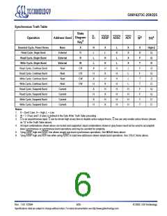
Burst Counter Sequences
Linear Burst Sequence
A[1:0] A[1:0] A[1:0] A[1:0]
Interleaved Burst Sequence
A[1:0] A[1:0] A[1:0] A[1:0]
1st address
2nd address
3rd address
4th address
00
01
10
11
01
10
11
00
10
11
00
01
11
00
01
10
1st address
2nd address
3rd address
4th address
00
01
10
11
01
00
11
10
10
11
00
01
11
10
01
00
Note:
The burst counter wraps to initial state on the 5th clock.
Note:
The burst counter wraps to initial state on the 5th clock.
BPR 1999.05.18
Rev: 1.03 7/2004
4/25
© 2002, GSI Technology
Specifications cited are subject to change without notice. For latest documentation see http://www.gsitechnology.com.

 GSI [ GSI TECHNOLOGY ]