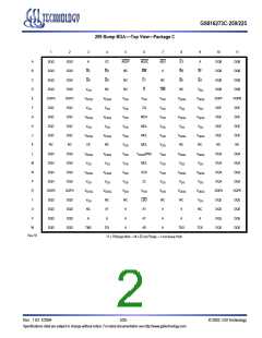
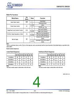
GS816273C-250/225
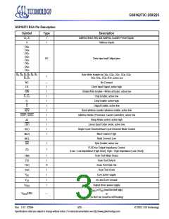
GS816273 BGA Pin Description
Symbol
A0, A1
A
Type
Description
I
I
Address field LSBs and Address Counter Preset Inputs.
Address Inputs
DQA
DQB
DQC
DQD
DQE
DQF
DQG
DQH
I/O
Data Input and Output pins
Byte Write Enable for DQA, DQB, DQC, DQD, DQE,
DQF, DQG, DQH I/Os; active low
BA, BB, BC,BD, BE, BF,
BG,BH
I
NC
CK
—
I
No Connect
Clock Input Signal; active high
I
Global Write Enable—Writes all bytes; active low
Chip Enable; active low
GW
I
E1, E3
E2
I
Chip Enable; active high
I
Output Enable; active low
G
I
Burst address counter advance enable; active low
Address Strobe (Processor, Cache Controller); active low
Sleep Mode control; active high
Linear Burst Order mode; active low
Single Cycle Deselect/Dual Cycle Deselect Mode Control
Must Connect High
ADV
ADSP, ADSC
ZZ
I
I
I
LBO
SCD
MCH
MCL
BW
I
I
Must Connect Low
I
I
Byte Enable; active low
FLXDrive Output Impedance Control
(Low = Low Impedance [High Drive], High = High Impedance [Low Drive])
ZQ
I
I
Scan Test Mode Select
Scan Test Data In
Scan Test Data Out
Scan Test Clock
TMS
TDI
O
I
TDO
TCK
V
I
Core power supply
DD
V
I
I
I/O and Core Ground
SS
V
Output driver power supply
DDQ
V
or V (must be tied high)
DDQ
DD
V
/DNU
—
or
DDQ
Do Not Use (must be left floating)
Rev: 1.03 7/2004
3/25
© 2002, GSI Technology
Specifications cited are subject to change without notice. For latest documentation see http://www.gsitechnology.com.

 GSI [ GSI TECHNOLOGY ]