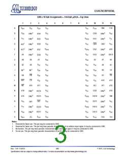
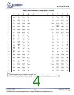
GS4576C09/18/36L
Operations
Initialization
A specific power-up and initialization sequence must be observed. Other sequences may result in undefined operations or
permanent damage to the device.
Power-up:
1. Apply power (VEXT, VDD, VDDQ, VREF, VTT) . Start clock after the supply voltages are stable. Apply VDD and VEXT before or
1
at the same time as VDDQ . Apply VDDQ before or at the same time as VREF and VTT. The chip starts internal initlization
2
only after both voltages approach their nominal levels. CK/CK must meet VID DC prior to being applied . Apply only
(
)
NOP commands to start. Ensuring CK/CK meet VID DC while loading NOP commands guarantees that the LLDRAM II
(
)
will not receive damaging commands during initialization.
2. Idle with continuing NOP commands for 200s (MIN).
3. Issue three or more consecutive MRS commands: two or more dummies plus one valid MRS. The consecutive MRS
commands will reset internal logic of the LLDRAM II. tMRSC does not need to be met between these consecutive
commands. Address pins should be held Low during the dummy MRS commands.
4. tMRSC after the valid MRS, issues an AUTO REFRESH command to all 8 banks in any order (along with 1024 NOP
commands) prior to normal operation. As always, tRC must be met between any AUTO REFRESH and any subsequent
valid command to the same bank.
Notes:
1. It is possible to apply VDDQ before VDD. However, when doing this, the DQs, DM, and all other pins with an output driver, will
go High instead of tri-stating. These pins will remain High until VDD is at the same level as VDDQ. Care should be taken to
avoid bus conflicts during this period.
2. If VID DC on CK/CK can not be met prior to being applied to the LLDRAM II, placing a large external resistor from CS to VDD
(
)
is a viable option for ensuring the command bus does not receive unwanted commands during this unspecified state.
Rev: 1.04 11/2013
7/62
© 2011, GSI Technology
Specifications cited are subject to change without notice. For latest documentation see http://www.gsitechnology.com.

 GSI [ GSI TECHNOLOGY ]