GS4576C09/18/36L
Ball Descriptions
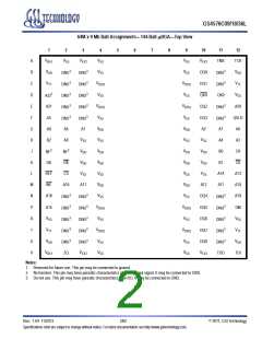
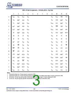
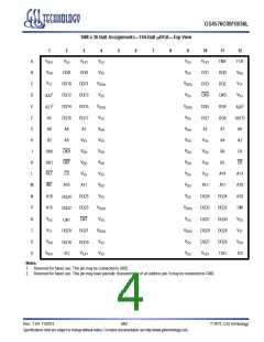
Symbol
Type
Description
Address Inputs—A0–A21 define the row and column addresses for Read and Write Operations. During
a Mode Register Set (MRS), the address inputs define the register settings. They are sampled at the
rising edge of CK.
A0–A21
Input
BA0–B2
CK, CK
Input
Input
Bank Address inputs—Select to which internal bank a command is being applied.
Input Clock—CK and CK are differential input clocks. Addresses and commands are latched on the
rising edge of CK. CK is ideally 180º out of phase with CK.
Chip Select—CS enables the command decoder when Low and disables it when High. When the
Input
Input
CS
command decoder is disabled, new commands are ignored, but internal operations continue.
Data Input—The DQ signals form the 36-bit data bus. During Read commands, the data is referenced to
DQ0–DQ35
both edges of QKx. During Write commands, the data is sampled at both edges of DK.
Input Data Clock—DK and DK are the differential input data clocks. All input data is referenced to both
edges of DK. DK is ideally 180º out of phase with DK. For the x36 device, DQ0– DQ17 are referenced to
DK0 and DK0 and DQ18–DQ35 are referenced to DK1 and DK1. For the x9 and x18 devices, all DQs
are referenced to DK and DK. All DKx and DKx pins must always be supplied to the device.
Input
Input
DK, DK
DM
Input Data Mask—The DM signal is the input mask signal for Write data. Input data is masked when DM
is sampled High. DM is sampled on both edges of DK (DK1 for the x36 configuration). Tie signal to
ground if not used.
IEEE 1149.1 clock input—This ball must be tied to V if the JTAG function is not used.
TCK
Input
Input
SS
IEEE 1149.1 test inputs—These balls may be left as no connects if the JTAG function is not used.
TMS, TDI
Command Inputs—Sampled at the positive edge of CK, WE and REF define (together with CS) the
Input
Input
WE, REF
command to be executed.
Input Reference Voltage—Nominally V /2. Provides a reference voltage for the input buffers.
V
DDQ
REF
External Impedance (25–60)—This signal is used to tune the device outputs to the system data bus
impedance. DQ output impedance is set to 0.2 * RQ, where RQ is a resistor from this signal to ground.
Connecting ZQ to GND invokes the Minimum Impedance mode. Connecting ZQ to V invokes the
I/O
ZQ
DD
Maximum Impedance mode. Refer to the Mode Register Definition diagrams (Mode Register Bit 8 (M8))
to activate or deactivate this function.
Output Data Clocks—QKx and QKx are opposite polarity, output data clocks. They are free running,
and during Reads, are edge-aligned with data output from the LLDRAM II. QKx is ideally 180º out of
phase with QKx. For the x36 device, QK0 and QK0 are aligned with DQ0–DQ17, and QK1 and QK1 are
aligned with DQ18–DQ35. For the x18 device, QK0 and QK0 are aligned with DQ0–DQ8, while QK1 and
QK1 are aligned with Q9–Q17. For the x9 device, all DQs are aligned with QK0 and QK0.
Output
QKx, QKx
Rev: 1.04 11/2013
5/62
© 2011, GSI Technology
Specifications cited are subject to change without notice. For latest documentation see http://www.gsitechnology.com.

 GSI [ GSI TECHNOLOGY ]