The serial data output circuits are shown in Figure 6. The
serial data outputs are designed to drive 50-75Ω controlled
impedance traces and can be easily connected to the
GS9028 cable driver as shown in Figure 7 and Figure 18.
Note that to output proper PECL signal levels, a resistor
must be connected between the two serial data outputs.
The S bit, used for single link data standards only, is
encoded in the TRSID word and indicates if the data is in
RGB or YCRCB format as per SMPTE RP174. In automatic
standard detection mode, the S bit can be read from the
HOSTIF read table. In manual mode, the S bit must be set
in the HOSTIF write table.
1.4 Automatic Standard Detection
1.5 Parallel Clock Output
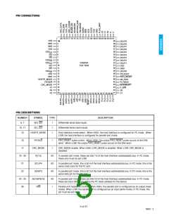
PIN
LOGIC OPR
HOST BIT
STD_SEL
STD[3:0]
S
PIN
LOGIC OPR
HOST BIT
PCLKOUT
STD[3:0]
The PCLKOUT pin provides the output parallel clock. All
synchronous I/O are timed relative to PCLKOUT. The
following listing shows which I/O's are synchronous and
which are not. Timing for synchronous outputs is shown in
Figure 3. Timing for synchronous inputs is shown in
Figure 2.
The device automatically detects the incoming video
standard. The detected standard is encoded on the
STD[3:0] pins and the HOSTIF read table bits as shown in
Table 1 and Table 3.
SYNCHRONOUS
FL[4:0]
ASYNCHRONOUS
P[7:5]
TABLE 1
STANDARD NAME
NTSC 4:2:2 Component with 13.5MHz Y sampling
NTSC Composite
STD[3:0]
0000
S[1:0]
SCL/P4
FIFO_RESET
DOUT[9:0]
F[2:0]
INTERRUPT
SDA/P3
0001
NTSC 4:2:2 16x9 Widescreen with 18MHz Y
sampling
0010
A[2:0]/P[2:0]
R/W
NTSC 4:4:4:4 Single Link with 13.5MHz Y sampling
PAL 4:2:2 Component with 13.5MHz Y sampling
PAL Composite
0011
0100
0101
0110
0111
V
H
A/D
ANC_DATA
BLANK_EN
F_R/W
CS
PAL 4:2:2 16x9 Widescreen with 18MHz Y sampling
PAL 4:4:4:4 Single Link with 13.5MHz Y sampling
FLAG_MAP
RESET
NO_EDH
STD[3:0]
TRS_ERROR
CRC_MODE
VBLANKS/L
HOSTIF_MODE
FIFOE/S
Noise immunity is included to ensure that momentary signal
corruption does not affect the automatic standards
detection function. This built in noise immunity results in
delayed detection time during power up and when
switching between standards. Delays range from as little as
eight lines when switching between component standards
to as much as four frames when switching between PAL
and NTSC standards. If this delay is intolerable, the user
can manually set the standard through the HOSTIF write
table. To set the standard manually, the STD_SEL bit must
be set HIGH and the S bit and STD[3:0] pins/HOSTIF bits
set accordingly. The default standard upon reset of the chip
is NTSC 4:2:2 component (13.5MHz Y sampling).
FLYWDIS
BYPASS_EDH
SDO_MODE
ANC_CHKSM
CLIP_TRS
9 of 31
19922 - 3

 GENNUM [ GENNUM CORPORATION ]