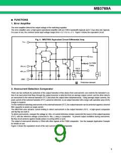
MB3769A
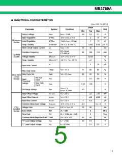
■ ELECTRICAL CHARACTERISTICS
(VCC=15V, TA=25°C)
Value
Parameter
Symbol
Condition
IREF = 1 mA
Unit
Min
4.9
-
Typ
5.0
2
Max
5.1
15
Output Voltage
VREF
V
Input Regulation
Load Regulation
Temp. Stability
∆ VRIN
∆ VRLD
∆ VRTEMP
ISC
12 V ≤ VCC ≤ 18 V
1 mA ≤ IREF ≤10 mA
-30 °C ≤ TA ≤ 85 °C
VREF = 0 V
mV
mV
Reference
Section
-
-1
-15
-
±200
40
±750 µV/ °C
Short Circuit Output Current
15
-
mA
RT=18 kΩ
CT=680 pF
Oscillator Frequency
fOSC
90
100
110
kHz
Oscillator
Section
Voltage Stability
Temp. Stability
∆ fOSCIN
12 V ≤ VCC ≤ 18 V
-
-
±0.03
±2
-
-
%
%
∆ fOSC /∆ T
-30 °C ≤ TA ≤ 85 °C
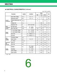
ID
-
2
10
µA
Input Bias Current
Dmax
Dset
VDO
Vd = 1.5 V
75
45
-
80
50
85
55
%
%
V
Max. Duty Cycle
Duty Cycle Set
0% Duty
Vd = 0.5 VREF
-
Dead -time
Control
Section
3.5
3.8
Input
Cycle
Threshold
Voltage
Max. Duty
Cycle
VDM
VDH
-
1.55
4.5
1.85
-
-
-
V
V
VCC= 7 V,
IDTC= -0.3 mA
Discharge Voltage
Input Offset Voltage
Input Offset Current
Input Bias Current
Common-Mode Input Voltage
Voltage Gain
VIO (OP)
IIO (OP)
IIR (OP)
VCM (OP)
AV (OP)
BW
V3 = 2.5 V
-
-
±2
±30
-0.3
-
±10
mV
nA
µA
V
V3 = 2.5 V
±300
V3 = 2.5 V
-1
-0.2
70
-
-
12 V ≤ VCC ≤ 18 V
0.5 V ≤ V3 ≤ 4 V
AV = 0dB
VCC -3
Error
Amplifier
Section
90
8
-
dB
MHz
V/µs
dB
V
Band Width
-
Slew Rate
SR
RL = 10 kΩ, AV = 0dB
VIN = 0 to 10 V
I3 = -2 mA
-
6
-
-
Common-Mode Rejection Rate CMR
65
4.0
-
80
4.6
0.1
“H” Level Output Voltage
“L” Level Output Voltage
VOH
VOL
-
I3 = 0.3 mA
0.5
V
5

 FUJITSU [ FUJITSU ]