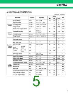
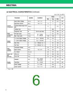
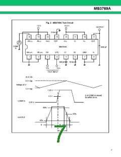
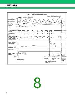
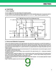
MB3769A
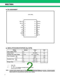
■ PIN ASSIGNMENT
(TOP VIEW)
+IN (OP)
-IN (OP)
1
2
3
+IN (C)
-IN (C)
VREF
OVP
16
15
14
FB
DTC
4
5
6
7
8
13
12
11
10
9
VCC
CT
RT
VZ
GND
VL
VH
OUT
■ ABSOLUTE MAXIMUM RATINGS (See NOTE)
Rating
Power Supply Voltage
Output Current
Symbol
Value
20
Unit
V
VCC
IOUT
Vin (OP)
PD
120 (660*)
mA
V
Operation Amp. Input Voltage
VCC + 0.3 (≤ 20)
1000**
mW
mW
°C
Power Dissipation: DIP
: FPT
PD
620***
TOP
-30 to +85
-30 to +75
-55 to +125
Operating Temp. : DIP
: FPT
TOP
°C
Storage Temp.
TSTG
°C
*
**
***
:
:
:
Duty ≤ 5%
TA = 25 °C
TA = 25 °C, FPT package is mounted on the epoxy board.
(4 cm x 4 cm x 0.15 cm)
NOTE : Permanent device damage may occur if the above Absolute Maximum Ratings are exceeded. Functional operation
should be restricted to the conditions as detailed in the operational sections data sheet. Exposure to absolute maximum
rating conditions for extended periods may affect device reliability.
2

 FUJITSU [ FUJITSU ]