DAC DK FPGA Adaptor
ꢀ
Features
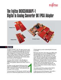
DAK DK FPGA Adaptor
V5-PCIE2 from HiTech Global
•
LVDS data interface for one (MB86065) or two
(MB86064) DAC cores
Loop Clock system for optimum timing
GPIO to FPGA
Support for single-supply operation: voltage regulators to
provide the DAC supply voltages (1.8V and 3.3V) using
the 5V supply for the V5-PCIE2 board
Socket to allow connection to the DK serial programming
header, eliminating the need for an external serial
programmer to program the DAC
•
•
•
•
•
Tri-mode Ethernet (10/100/1000)
4-lane PCI Express End-Point connector (upstream)
DDR2 SO-DIMM socket (up to 4GB)
512Mb DDR3 component
128Mb platform Flash XL for configuration and user
flash
On board clocking
Many Virtex 5 parts such as the XC5VLX50T and
XC5VFX100T are available
Programmable over JTAG or via the on-board 128Mb
Flash, which removes the need to reprogram the device at
power on. Programming is performed via a Xilinx USB
programming cable.
•
•
•
•
•
•
•
ꢀ
Ordering Information
Part
Order Reference
DAC DK FPGA adaptor
DKXC5VADAPT-1
Complete development kit (including
evaluation board with device fitted, PC
USB programming cable, control
software and user manual)
DK86064/65-2
HTG-V5-DDR3-PCIE2-####
CONTACT HITECH GLOBAL
(www.HiTechGlobal.com)
HiTech Global V5-PCIE2 FPGA
Development Platform
HW-USB-II
CONTACT XILINX
(www.Xilinx.com)
Xilinx USB Programming Cable
FUJITSU MICROELECTRONICS AMERICA, INC.
Corporate Headquarters
© 2009 Fujitsu Microelectronics America, Inc.
1250 E. Arques Avenue, M/S 333, Sunnyvale, CA 94085-5401
Tel: (800) 866-8608 Fax: (408) 737-5999
E-mail: inquiry@fma.fujitsu.com Web Site: http://us.fujitsu.com/micro
All company and product names are trademarks or
registered trademarks of their respective owners.
Printed in the U.S.A. EPS-FS-21355-11/2009

 FUJITSU [ FUJITSU ]