The Fujitsu DKXC5VADAPT-1
Digital to Analog Converter DK FPGA Adaptor
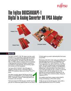
Adaptor Front
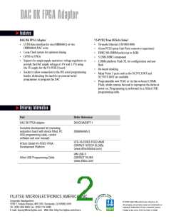
Complete System
Adaptor Back
ꢀ
Description
The DKXC5VADAPT-1 DAC DK adaptor provides a quick
and effective way to demonstrate a high-speed data interface
to the Fujitsu DK86064 and DK86065 high-performance
DAC development kits. The adaptor directly connects the
DKs to an FBGA platform (a popular device for interfacing
to high-speed data converters), providing a relatively low-
cost platform for high-speed logic, data processing, digital
data interfaces and clock management.
All clock signals are routed to dedicated global clock inputs
on the FPGA.
Maintaining valid clock-to-data timing can be difficult when
using high-speed data converters. The MB86064/65 DACs
solve this problem with a Loop Clock system. The Loop
Clock is generated in sync with the DAC data at the FPGA
output. This clock is passed through a user-programmable
delay in the DAC and then routed back to the FPGA’s PLL
feedback input. Altering the delays in the divided clock or
Loop Clock signals allows the user to advance or retard data
timings in order to find the optimum data eye. Once
calibrated, the system automatically compensates for the
effects of device-to-device variations in phase, voltage and
temperature (PVT).
The Fujitsu DKXC5VADAPT-1 DAC DK adaptor is
designed to interface directly to the HiTech Global V5-
®
PCIE2 FPGA platform, which uses the Xilinx Virtex™-5
device.
The adaptor provides a physical link between the data
headers on the DK86064/65-2 and the HiTech Global V5-
®
PCIE2. Underneath, 6 Samtec sockets plug directly into
The complete system forms a compact solution ideal for
testing and developing an FPGA-DAC interface.
the headers on the two boards.
The board connects 28 LVDS data pairs, the DAC loop clock
pairs and two divided clock signals between the two boards.
To help users get started with the system, Fujitsu offers a
sample implementation for the FPGA interface.

 FUJITSU [ FUJITSU ]