FT4232H QUAD HIGH SPEED USB TO MULTIPURPOSE UART/MPSSE IC
Datasheet
Version 2.4
Document No.: FT_000060 Clearance No.: FTDI#78
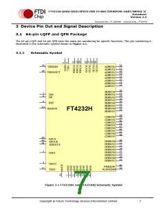
3.1.3
Common Pins
The operation of the following FT4232H pins are the same regardless of the configured mode:-
Pin No.
Name
Type
Description
POWER
Input
12,37,64
VCORE
+1.8V input. Core supply voltage input.
POWER
Input
+3.3V input. I/O interface power supply input. Failure to connect all
VCCIO pins will result in failure of the device.
20,31,42,56
9
VCCIO
VPLL
POWER
Input
+3.3V input. Internal PHY PLL power supply input. It is recommended
that this supply is filtered using an LC filter.
+3.3V Input. Internal USB PHY power supply input. Note that this
cannot be connected directly to the USB supply. A +3.3V regulator
must be used. It is recommended that this supply is filtered using an LC
filter.
POWER
Input
4
VPHY
POWER
Input
50
49
10
VREGIN
VREGOUT
AGND
+3.3V Input. Integrated 1.8V voltage regulator input.
POWER
Output
+1.8V Output. Integrated voltage regulator output. Connect to VCORE
with 3.3uF filter capacitor.
POWER
Input
0V Analog ground.
0V Ground input.
1,5,11,15,
POWER
Input
GND
25,35,47,51
Table 3.2 Power and Ground for 64-pin QFN and LQFP package
Pin No.
Name
OSCI
OSCO
REF
Type
INPUT
OUTPUT
INPUT
I/O
Description
2
3
Oscillator input.
Oscillator output.
6
Current reference – connect via a 12K Ohm resistor @ 1% to GND.
USB Data Signal Minus.
7
DM
8
I/O
USB Data Signal Plus.
DP
13
14
TEST
INPUT
INPUT
IC test pin – for normal operation should be connected to GND.
Reset input (active low).
RESET#
PWREN#
Active low power-enable output.
PWREN# = 0: Normal operation.
60
36
OUTPUT
OUTPUT
PWREN# =1: USB SUSPEND mode or device has not been configured.
This can be used by external circuitry to power down logic when device
is in USB suspend or has not been configured.
SUSPEND#
Active low when USB is in suspend mode.
Table 3.3 Common Function pins for 64-pin QFN and LQFP Package
Copyright © Future Technology Devices International Limited
9

 FTDI [ FUTURE TECHNOLOGY DEVICES INTERNATIONAL LTD. ]