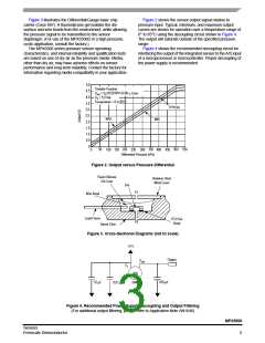
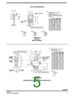
Figure 3 illustrates the Differential/Gauge basic chip
carrier (Case 867). A fluorosilicone gel isolates the die
surface and wire bonds from the environment, while allowing
the pressure signal to be transmitted to the sensor
diaphragm. (For use of the MPX5500D in a high pressure,
cyclic application, consult the factory.)
Figure 2 shows the sensor output signal relative to
pressure input. Typical, minimum, and maximum output
curves are shown for operation over a temperature range of
0° to 85°C using the decoupling circuit shown in Figure 4.
The output will saturate outside of the specified pressure
range.
The MPX5500 series pressure sensor operating
Figure 4 shows the recommended decoupling circuit for
interfacing the output of the integrated sensor to the A/D input
of a microprocessor or microcontroller. Proper decoupling of
the power supply is recommended.
characteristics, and internal reliability and qualification tests
are based on use of dry air as the pressure media. Media,
other than dry air, may have adverse effects on sensor
performance and long-term reliability. Contact the factory for
information regarding media compatibility in your application.
5.0
Transfer Function:
4.5
V
V
out = VS*(0.0018*P+0.04) ± Error
S = 5.0 Vdc
4.0
3.5
3.0
2.5
Temperature = 0 to 85°C
TYPICAL
MAX
MIN
2.0
1.5
1.0
0.5
0
50 100
200 250
350 400
500 550
0
150
300
450
Differential Pressure (kPa)
Figure 2. Output versus Pressure Differential
Fluoro Silicone
Stainless Steel
Die Coat
Metal Cover
Die
P1
Wire Bond
Lead Frame
RTV Die
Bond
P2
Epoxy Case
Figure 3. Cross-Sectional Diagrams (not to scale)
+5 V
Output
Vout
Vs
IPS
1.0 µF
GND
470 pF
0.01 µF
Figure 4. Recommended Power Supply Decoupling and Output Filtering
(For additional output filtering, please refer to Application Note AN1646)
MPX5500
Sensors
Freescale Semiconductor
3

 FREESCALE [ Freescale ]