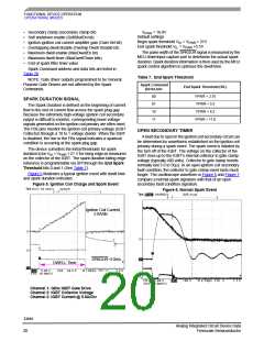
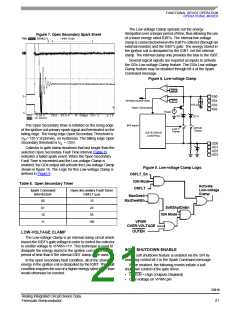
FUNCTIONAL DEVICE OPERATION
OPERATIONAL MODES
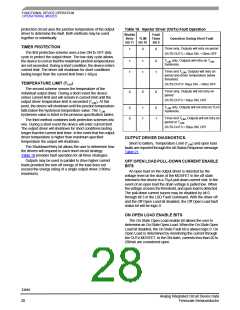
GENERAL PURPOSE GATE DRIVER MODE
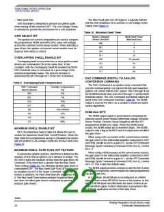
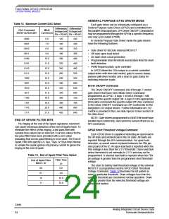
Table 12. Maximum Current DAC Select
Each gate driver can be individually configured as a
General Purpose Gate Driver (GPGD) and controlled from
the parallel GINx input pins, SPI Driver ON/OFF Command or
may be programmed through the SPI for a specific frequency
and duty cycle output (PWM).
Differential Differential
Voltage (mV Voltage (mV
Rs = 20 mΩ Rs = 40 mΩ
DAC Command
Bit<b11,b10,b9,b8>
MAXI
Current (A)
0000
0001
0010
0011
0100
0101
0110
0111
1000
1001
1010
1011
1100
1101
1110
1111
6.0
7.0
120
140
160
180
200
220
240
260
280
300
320
340
360
380
400
420
240
280
320
360
400
440
480
520
560
600
640
680
720
760
800
840
In General Purpose Gate Driver mode the gate drivers
have the following features:
8.0
• Gate driver for discrete external MOSFET
• Off state open load detect
• On state short circuit protection
• Programmable drain threshold and duration timer for short
fault detection
9.0
10.0
11.0
12.0
13.0
14.0
15.0
16.0
17.0
18.0
19.0
20.0
21.0
• PWM frequency/duty cycle controller
In GPGD Mode the GDx output is a current controlled
output driver with slew rate control, gate to source clamp,
passive pull-down resistor and a drain to gate clamp for
switching inductive loads.
Driver ON/OFF Command
The Driver ON/OFF Command, bits 4 through 7 control
gate drivers that have been Mode Select Command
programmed as GPGD. A logic 1 in bits 4 through 7 will
command the specific output ON. A logic 0 in the appropriate
bit location commands the specific output Off. Also contained
in the Driver ON/OFF Command are SPI control bits for the
integrated LSD output drivers. Further information on LSD
control is provided in the Low Side Injector Driver section of
the data sheet.
NOTE: Gate drivers programmed to IGNITION mode have
parallel input control only, and cannot be turned off and on via
SPI commands.
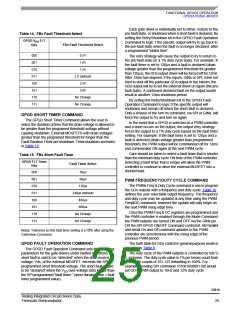
END OF SPARK FILTER BITS
The ringing at the end of the Spark signatures waveform
can cause erroneous detection of the End of Spark event. To
eliminate the effect of this ringing, a low pass filter with
variable time values can be selected. Four time values for the
low pass filter have been provided with a zero value
indicating that no low pass filtering is to be used. The End of
Spark Filter bits specify a 0, 4µs, 16µs, or 32µs time interval
to sample the spark ignition coil primary current to ignore the
ringing at the end of spark.
GPGD Short Threshold Voltage Command
Each GPGD driver is capable of detecting an open load in
the off state and shorted load in the on state. All faults are
reported through the SPI communication. For open load
detection, a current source is placed between the FBx pin
and ground of the IC. An open load fault is reported when the
FBx voltage is less than the 2.5 V threshold. Open load fault
detect threshold is set internally to 2.5 V and may not be
programmed. A shorted load fault is reported when the FBx
pin voltage is greater than the programmed short threshold
voltage.
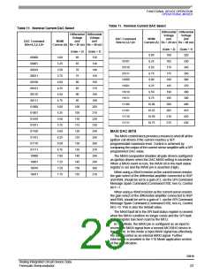
Table 13. End of Spark Filter Time Select
Filter Time
End of Spark Filter
Bits<1, 0>
µs
The short to battery fault threshold voltage of the external
MOSFET is programmed via the GPGD Short Threshold
Voltage Command. Table 14 illustrates the bit pattern to
select a particular threshold. Drain voltages less than the
selected threshold are considered normal operation. Drain
voltages greater than the selected threshold voltage are
considered faulted.
00
01
10
11
0.0
4.0
16.0
32.0
33810
Analog Integrated Circuit Device Data
Freescale Semiconductor
24

 FREESCALE [ Freescale ]