Freescale Semiconductor, Inc.
Table A-4 Control Timing
VDD = 5.0 Vdc ± 5%, VSS = 0 Vdc, TA = TL to TH
Characteristic
Symbol
2.0 MHz
3.0 MHz
4.0 MHz
Unit
Min Max Min Max Min Max
Frequency of Operation
f
dc
500
—
2.0
—
dc
333
—
3.0
—
dc
250
—
4.0 MHz
ns
o
E-Clock Period
t
—
cyc
Crystal Frequency
f
8.0
8.0
—
12.0
12.0
—
16.0 MHz
16.0 MHz
XTAL
External Oscillator Frequency
4 f
dc
dc
dc
o
Processor Control Setup Time
t
t
175
133
113
—
ns
PCSU
= 1/4 t + 50 ns
PCSU
cyc
Reset Input Pulse Width (Notes 2, 3)
(To Guarantee External Reset Vector)
PW
RSTL
16
1
—
—
16
1
—
—
16
1
—
—
t
t
cyc
cyc
(Minimum Input Time;
Can Be Preempted by Internal Reset)
Mode Programming Setup Time
t
2
—
—
—
2
—
—
—
2
—
—
—
t
MPS
cyc
Mode Programming Hold Time
t
10
10
10
ns
ns
MPH
Interrupt Pulse Width, IRQ Edge-Sensitive Mode
PW
520
353
270
IRQ
PW
= t + 20 ns
IRQ
cyc
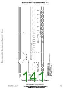
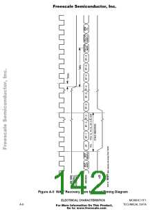
Wait Recovery Startup Time
t
—
4
—
4
—
4
t
cyc
WRS
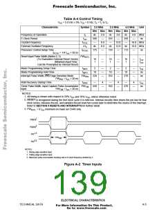
Timer Pulse Width, Input Capture Pulse Accumulator PW
520
—
353
—
270
—
ns
TIM
Input
PW
= t + 20 ns
TIM cyc
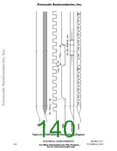
NOTES:
1. All timing is shown with respect to 20% V and 70% V , unless otherwise noted.
DD
DD
2. RESET is recognized during the first clock cycle it is held low. Internal circuitry then drives the pin low for four
clock cycles, releases the pin, and samples the pin level two cycles later to determine the source of the interrupt.
Refer to SECTION 5 RESETS AND INTERRUPTS for further detail.
3. PW
= 8 t minimum on mask set C94R only.
cyc
RSTL
1
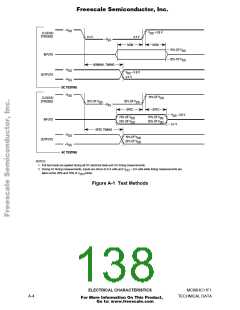
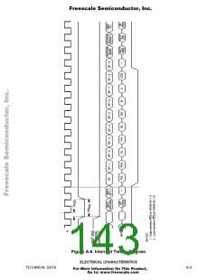
PA[3:0]
2
PA[3:0]
1,3
PA7
PA7
PW
TIM
2,3
NOTES:
1. Rising edge sensitive input.
2. Falling edge sensitive input.
3. Maximum pulse accumulator clocking rate is E-clock frequency divided by 2.
Figure A-2 Timer Inputs
ELECTRICAL CHARACTERISTICS
TECHNICAL DATA
A-5
For More Information On This Product,
Go to: www.freescale.com

 FREESCALE [ Freescale ]