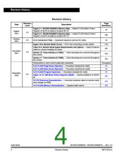
Revision History
Revision History
Revision
Level
Page
Number(s)
Date
Description
Figure 2-1. MC68HC908MR32 Memory Map — Added FLASH Block Protect
Register (FLBPR) at address location $FF7E
29
August,
3.0
2001
Figure A-1. MC68HC908MR16 Memory Map — Added FLASH Block Protect
306
Register (FLBPR) at address location $FF7E
October,
4.0
3.3.3 Conversion Time — Reworked equations and text for clarity.
50
2001
Figure 18-8. Monitor Mode Circuit — PTA7 and connecting circuitry added
279
281
Table 18-2. Monitor Mode Signal Requirements and Options — Switch locations
added to column headings for clarity
December,
5.0
Section 16. Timer Interface A (TIMA) — Timer discrepancies corrected throughout
this section.
2001
233
255
Section 17. Timer Interface B (TIMB) — Timer discrepancies corrected throughout
this section.
Reformatted to meet current publication standards
Throughout
2.8.2 FLASH Page Erase Operation — Procedure reworked for clarity
2.8.3 FLASH Mass Erase Operation — Procedure reworked for clarity
2.8.4 FLASH Program Operation — Procedure reworked for clarity
42
42
43
November,
6.0
Figure 14-14. SIM Break Status Register (SBSR) — Clarified definition of SBSW
bit.
2003
207
19.5 DC Electrical Characteristics — Corrected maximum value for monitor mode
entry voltage (on IRQ)
291
292
19.6 FLASH Memory Characteristics — Updated table entries
Data Sheet
4
MC68HC908MR32 • MC68HC908MR16 — Rev. 6.0
MOTOROLA
Revision History

 FREESCALE [ Freescale ]