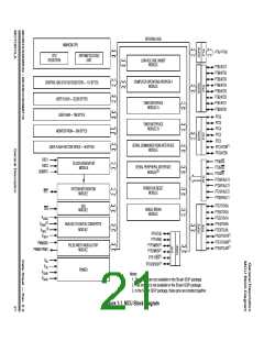
General Description
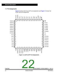
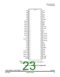
Pin Assignments
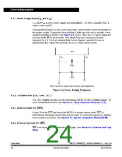
1.4.5 CGM Power Supply Pins (VDDA and VSSAD
)
VDDA and VSSAD are the power supply pins for the analog portion of the clock
generator module (CGM). Decoupling of these pins should be per the digital
supply. See Section 4. Clock Generator Module (CGM).
1.4.6 External Filter Capacitor Pin (CGMXFC)
CGMXFC is an external filter capacitor connection for the CGM. See Section 4.
Clock Generator Module (CGM).
1.4.7 Analog Power Supply Pins (VDDAD and VSSAD
)
VDDAD and VSSAD are the power supply pins for the analog-to-digital converter.
Decoupling of these pins should be per the digital supply. See Section 3.
Analog-to-Digital Converter (ADC).
1.4.8 ADC Voltage Decoupling Capacitor Pin (VREFH
)
VREFH is the power supply for setting the reference voltage. Connect the VREFH pin
to the same voltage potential as VDDAD. See Section 3. Analog-to-Digital
Converter (ADC).
1.4.9 ADC Voltage Reference Low Pin (VREFL
)
VREFL is the lower reference supply for the ADC. Connect the VREFL pin to the
same voltage potential as VSSAD. See Section 3. Analog-to-Digital Converter
(ADC).
1.4.10 Port A Input/Output (I/O) Pins (PTA7–PTA0)
PTA7–PTA0 are general-purpose bidirectional input/output (I/O) port pins. See
Section 10. Input/Output (I/O) Ports (PORTS).
1.4.11 Port B I/O Pins (PTB7/ATD7–PTB0/ATD0)
Port B is an 8-bit special function port that shares all eight pins with the
analog-to-digital converter (ADC). See Section 3. Analog-to-Digital Converter
(ADC) and Section 10. Input/Output (I/O) Ports (PORTS).
1.4.12 Port C I/O Pins (PTC6–PTC2 and PTC1/ATD9–PTC0/ATD8)
PTC6–PTC2 are general-purpose bidirectional I/O port pins (see Section 10.
Input/Output (I/O) Ports (PORTS)). PTC1/ATD9–PTC0/ATD8 are special
function port pins that are shared with the analog-to-digital converter (ADC). See
Section 3. Analog-to-Digital Converter (ADC) and Section 10. Input/Output
(I/O) Ports (PORTS).
MC68HC908MR32 • MC68HC908MR16 — Rev. 6.0
MOTOROLA
Data Sheet
25
General Description

 FREESCALE [ Freescale ]