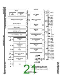
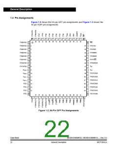
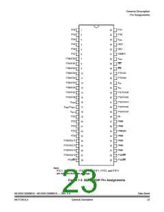
General Description
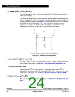
1.4.1 Power Supply Pins (VDD and VSS
)
VDD and VSS are the power supply and ground pins. The MCU operates from a
single power supply.
Fast signal transitions on MCU pins place high, short-duration current demands on
the power supply. To prevent noise problems, take special care to provide power
supply bypassing at the MCU as Figure 1-4 shows. Place the C1 bypass capacitor
as close to the MCU as possible. Use a high-frequency-response ceramic
capacitor for C1. C2 is an optional bulk current bypass capacitor for use in
applications that require the port pins to source high-current levels.
MCU
VDD
VSS
C1
0.1 µF
+
C2
1–10 µF
VDD
Note: Component values shown represent typical applications.
Figure 1-4. Power Supply Bypassing
1.4.2 Oscillator Pins (OSC1 and OSC2)
The OSC1 and OSC2 pins are the connections for the on-chip oscillator circuit. For
more detailed information, see Section 4. Clock Generator Module (CGM).
1.4.3 External Reset Pin (RST)
A logic 0 on the RST pin forces the MCU to a known startup state. RST is
bidirectional, allowing a reset of the entire system. It is driven low when any internal
reset source is asserted. See Section 14. System Integration Module (SIM).
1.4.4 External Interrupt Pin (IRQ)
IRQ is an asynchronous external interrupt pin. See Section 8. External Interrupt
(IRQ).
Data Sheet
24
MC68HC908MR32 • MC68HC908MR16 — Rev. 6.0
General Description
MOTOROLA

 FREESCALE [ Freescale ]