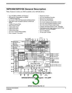
56F8366/56F8166 General Description
Note: Features in italics are NOT available in the 56F8166 device.
• Up to 60 MIPS at 60MHz core frequency
• Temperature Sensor
• DSP and MCU functionality in a unified,
C-efficient architecture
• Access up to 1MB of off-chip program and data memory
• Chip Select Logic for glueless interface to ROM and
SRAM
• 512KB of Program Flash
• 4KB of Program RAM
• 32KB of Data Flash
• 32KB of Data RAM
• 32KB of Boot Flash
• Up to two 6-channel PWM modules
• Four 4-channel, 12-bit ADCs
• Up to two Quadrature Decoders
• Optional On-Chip Regulator
• Up to two FlexCAN modules
• Two Serial Communication Interfaces (SCIs)
• Up to two Serial Peripheral Interfaces (SPIs)
• Up to four General Purpose Quad Timers
• Computer Operating Properly (COP) / Watchdog
• JTAG/Enhanced On-Chip Emulation (OnCE™) for
unobtrusive, real-time debugging
• Up to 62 GPIO lines
• 144-pin LQFP Package
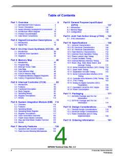
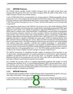
OCR_DIS
EMI_MODE
V
2
V
VDD
VSS VDDA
VSSA
RSTO
PP
CAP
EXTBOOT
5
RESET
4
7
5
2
6
6
JTAG/
EOnCE
Port
PWM Outputs
Digital Reg
Analog Reg
PWMA
3
3
Current Sense Inputs
or GPIOC
Low Voltage
Supervisor
16-Bit
56800E Core
Fault Inputs
Program Controller
and
Hardware Looping Unit
Address
Generation Unit
Data ALU
Bit
Manipulation
Unit
PWM Outputs
PWMB
16 x 16 + 36 -> 36-Bit MAC
Three 16-bit Input Registers
Four 36-bit Accumulators
3
4
Current Sense Inputs
or GPIOD
Fault Inputs
PAB
PDB
CDBR
CDBW
4
4
AD0
ADCA
AD1
R/W Control
5
Memory
Program Memory
256K x 16 Flash
2K x 16 RAM
VREF
XDB2
XAB1
XAB2
6
A0-5 or GPIOA8-13
A6-7 or GPIOE2-3
4
4
External
Address Bus
Switch
AD0
AD1
2
8
ADCB
A8-15 or GPIOA0-7
GPIOB0 or A16
System Bus
Control
Boot ROM
16K x 16 Flash
PAB
Temp_Sense
PDB
7
9
Quadrature
Decoder 0 or
Quad
Timer A or
GPIOC
External Data
Bus Switch
D0-6 or GPIOF9-15
D7-15 or GPIOF0-8
CDBR
CDBW
Data Memory
16K x 16 Flash
16K x 16 RAM
4
WR
RD
Bus Control
Quadrature
Decoder 1 or
Quad
Timer B or
SPI1 or
PS / CS0 (GPIOD8)
DS / CS1 (GPIOD9)
4
IPBus Bridge (IPBB)
GPIO or
EMI CS or
FlexCAN2
GPIOD0 (CS2 or CAN2_TX)
GPIOD1 (CS3 or CAN2_RX)
GPIOC
Peripheral
Device Selects
RW
IPAB
IPWDB
IPRDB
Quad
Timer C or
GPIOE
Control
Decoding
Peripherals
Quad
Timer D or
GPIOE
2
2
Clock
resets
PLL
FlexCAN
P
O
R
System
Integration
Module
O
SPI0 or
GPIOE
SCI1 or
GPIOD
SCI0 or
GPIOE
COP/
Interrupt
Clock
XTAL
S
Generator
C
Watchdog Controller
EXTAL
4
2
2
IRQA IRQB
CLKMODE
CLKO
56F8366/56F8166 Block Diagram - 144 LQFP
56F8366 Technical Data, Rev. 2.0
Freescale Semiconductor
Preliminary
3

 FREESCALE [ Freescale ]