Freescale Semiconductor, Inc.
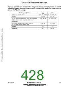
The V
and GND pins are separated into groups to help electrically isolate the different
CC
output drivers of the MC68340. These groups are shown in the following table for the RP
suffix package.
Pin Group — RP Suffix
Address Bus, Function Codes
V
GND
CC
D2, G3, K3, K14, M3 D3, G2, J3, K13, M2
Data Bus
C14, F13
D13, G13
AS, BG, CLKOUT, DS, FREEZE, HALT, IFETCH, IPIPE,
MODCK, RESET, RMC, R/W, SIZx, TDO, TOUT1, Internal
Logic
M13, N4, N9, P9
N3, N7, N10, N13
CS≈, DACK≈, DONE≈, IRQ≈, RTS≈, R≈RDYA, TOUT2,
TxDx, T≈RDYA, Internal Logic
B11, C4, C7
C5, C8, C11
Oscillator
N8
P7
—
Internal Only
H3, H13
MOTOROLA
MC68340 USER’S MANUAL
12-5
For More Information On This Product,
Go to: www.freescale.com

 FREESCALE [ Freescale ]