Freescale Semiconductor, Inc.
PLL Tuned UHF Transmitter Module
When connected to V , the bias current on the BS pin is in the range
CC
of 26 µA. To avoid any excessive battery current in sleep mode, tying the
BS pin to the PLLEN pin is recommended.
16.5 Output Stage
The integrated RF module offers a single-ended configuration allowing
a more efficient use of the battery current in the case of low-impedance
antennas.
The output stage is a square wave switched current source. Harmonics
will be present in the output current drive; their radiated absolute level
depends on the antenna characteristics and output power. Typical
application has demonstrated compliance to the European
Telecommunications Standards Institute (ETSI) standard. To remain
within the admissible voltage range, the output voltage is limited to V
CC
+/– 2 V .
PP
A resistor connected to the REXT pin controls the output power allowing
a tradeoff between radiated power and current consumption.
Furthermore, the output power will be gradually reduced when the
battery voltage decreases below a defined threshold (see 16.8 Power
Management).
16.6 Modulation
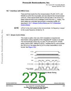
On-off keying (OOK) and FSK modulation are performed internally, the
modulation mode being selected through the MODE pin as described in
16.7.1 Simple Control Mode. No extra components are required for
OOK. An external RC filter is required at the PFD pin to reduce the loop
bandwidth in FSK mode. FSK frequency deviation is accurately defined
by dividing down the XTAL frequency.
The exact frequency deviation is equal to XTAL frequency divided by
128, giving a deviation of approximately:
•
•
±106 kHz in the 434/868-MHz bands
±77 kHz in the 315-MHz band
Advance Information
224
MC68HC908RFRK2
MOTOROLA
PLL Tuned UHF Transmitter Module
For More Information On This Product,
Go to: www.freescale.com

 FREESCALE [ Freescale ]