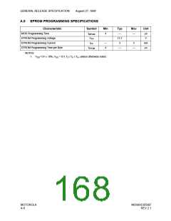
GENERAL RELEASE SPECIFICATION
August 27, 1998
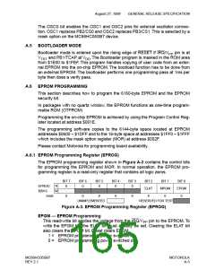
MPGM — Mask Option Register (MOR) Programming
This read/write bit applies programming power from the IRQ/V
MOR. Reset clears MPGM.
pin to the
PP
1 = MOR programming power switched on.
0 = MOR programming power switched off.
ELAT — EPROM Bus Latch
This read/write bit configures address and data buses for programming the
EPROM array. EPROM data cannot be read when ELAT is set. Clearing the
ELAT bit also clears the EPGM bit. Reset clears ELAT.
1 = Address and data buses configured for EPROM programming of the
array. The address and data bus are latched in the EPROM array
when a subsequent write to the array is made. Data in the EPROM
array cannot be read.
0 = Address and data buses configured for normal operation.
Whenever the ELAT bit is cleared the EPGM bit is also cleared. Both the EPGM
and the ELAT bit cannot be set using the same write instruction. Any attempt to
set both the ELAT and EPGM bit on the same write instruction cycle will result in
the ELAT bit being set and the EPGM bit being cleared.
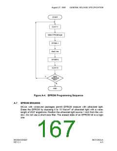
A.6.2 Programming Sequence
The EPROM programming sequence is:
1. Set the ELAT bit in the EPROG register.
2. Write the desired data to the desired EPROM address.
3. Set the EPGM bit in the EPROG register for the specified programming
time (t
).
EPGM
4. Clear the EPGM bit
5. Clear the ELAT bit
The last two steps must be performed with separate CPU writes.
CAUTION
It is important to remember that an external programming voltage
must be applied to the V pin while programming, but it should be
PP
equal to V during normal operations.
DD
Figure A-4 shows the flow required to successfully program the EPROM.
MOTOROLA
A-4
MC68HC05SB7
REV 2.1

 FREESCALE [ Freescale ]