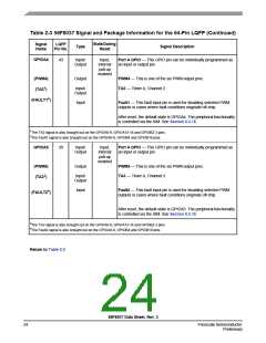
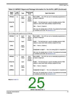
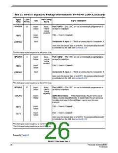
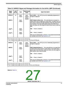
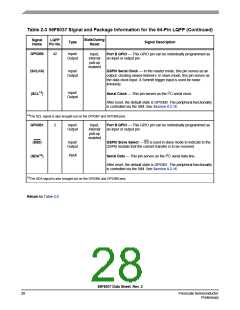
Table 2-3 56F8037 Signal and Package Information for the 64-Pin LQFP (Continued)
Signal
Name
LQFP
Pin No.
StateDuring
Reset
Type
Signal Description
GPIOB0
42
Input/
Output
Input,
internal
pull-up
enabled
Port B GPIO — This GPIO pin can be individually programmed as
an input or output pin.
(SCLK0)
Input/
Output
QSPI0 Serial Clock — In the master mode, this pin serves as an
output, clocking slaved listeners. In slave mode, this pin serves as
the data clock input. A Schmitt trigger input is used for noise
immunity.
(SCL14
)
Serial Clock — This pin serves as the I2C serial clock.
Input/
Output
After reset, the default state is GPIOB0. The peripheral functionality
is controlled via the SIM. See Section 6.3.16.
14The SCL signal is also brought out on the GPIOB7 and GPIOB8 pins.
GPIOB1
2
Input/
Output
Input,
internal
pull-up
enabled
Port B GPIO — This GPIO pin can be individually programmed as
an input or output pin.
(SS0)
Input/
QSPI0 Slave Select — SS is used in slave mode to indicate to the
Output
QSPI0 module that the current transfer is to be received.
(SDA15
)
Serial Data — This pin serves as the I2C serial data line.
Input
After reset, the default state is GPIOB1. The peripheral functionality
is controlled via the SIM. See Section 6.3.16.
15The SDA signal is also brought out on the GPIOB6 and GPIOB9 pins.
Return to Table 2-2
56F8037 Data Sheet, Rev. 3
28
Freescale Semiconductor
Preliminary

 FREESCALE [ Freescale ]