PIN CONNECTIONS
PIN CONNECTIONS
29
17
16
15
14
13
12
11
10
9
GND
GND
VB+
30
31
32
33
34
35
36
37
38
39
VB+
VB+
VB+
DR2B1
DR2SENSE1
DR2A1
VB+
DR2B2
DR2SENSE2
DR2A2
VB+
V1_SWITCH
DR1_MODE
V1_FB
GND
V2_SWITCH
DR2_MODE
V2_FB
8
7
GND
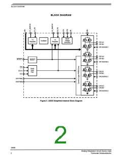
Figure 3. 34920 Pin Connections
Table 1. 34920 Pin Definitions
Pin Number Pin Name
Formal Name
Definition
Pin to connect to V capacitor.
Vb
1
2
3
4
5
VB
CP2
Output pin to V
Vb
Pin for boost generator switch capacitor.
Pin for boost generator switch capacitor.
Active low Reset output.
Capacitor to CP1
Capacitor to CP2
Reset Output
CP1
RESET
VCC
V
power input for internal use. The 34920 accepts either 3.3 V ±10% or
V
Supply Voltage
CC
CC
5.0 V ±5% for its logic voltage.
Ground connections for digital IC circuitry.
6, 7, 17, 18,
GND
Substrate Ground
28, 29, 39, 40
Voltage feedback for the V1 regulator.
8
9
V1_FB
V1 Regulator Feedback Input
Mode Select for Driver 1
Selects operational mode of Driver 1; Step = 1/DC = 0.
Switching output for V1 regulator.
DR1_MODE
10
V1_SWITCH Internal MOSFET Source for V1
Regulator
High-voltage supply for motors and regulators.
11, 15, 16,
VB+
VB+ (Bulk) Supply Voltage
23, 30, 31, 35
Motor driver output.
12
13
14
19
20
DR2A1
DR2SENSE1
DR2B1
Driver 2, Bridge 1, Output A
Driver 2, Bridge 1, I Sense
Driver 2, Bridge 1, Output B
Driver 1, Bridge 1, Output A
Driver 1, Bridge 1, I Sense
Current sense for current mode.
Motor driver output.
Motor driver output.
DR1A1
Current sense for current mode.
DR1SENSE1
34920
Analog Integrated Circuit Device Data
Freescale Semiconductor
3

 FREESCALE [ Freescale ]