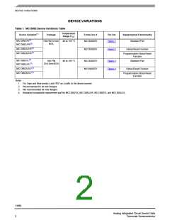
PIN CONNECTIONS
Table 2. 13892 Pin Definitions
A functional description of each pin can be found in the Functional Pin Description section beginning on page 32.
Pin Number
Pin Number on
the 13982VL
12x12 mm
on the
13982VK
7x7 mm
Rating
(V)
Pin Name
Pin Function
Formal Name
Definition
Output regulator for USB PHY
Input regulator VUSB2
Switcher BST input
A1, A2, B1
A2
A3
A5
VUSB2
VINUSB2
SWBSTIN
3.6
5.5
5.5
Output
Power
Power
USB 2 Supply
A3
A4
USB 2 Supply Input
Switcher Boost Power
Input
Ground for switcher BST
Ground for serial LED drive
Do NOT connect
A5
A6
A7
A8
D5
D8
A7
A8
GNDSWBST
GNDBL
NC
-
-
Ground
Ground
-
Switcher Boost Ground
Backlight LED Ground
No Connect
-
USB LBP mode, normal mode, test mode
selection & anti-fuse bias
MODE
9.0
Input
Mode Configuration
Regulated supply output for the IC analog
core circuitry
A9
A9
VCORE
BATT
3.6
5.5
Output
Input
Core Supply
1. Battery positive terminal
A10
A10
Battery Connection
2. Battery current sensing point 2
3. Battery supply voltage sense
1. Charger input
A11
A11
CHRGRAW
20
I/O
Charger Input
2. Output to battery supplied accesories
Driver output for charger path FETs M2
General purpose output 1
A12, A13, B13
B2
A12
B2
CHRGCTRL2
GPO1
5.5
3.6
Output
Output
Charger Control 2
General Purpose
Output 1
Switcher 2 DVS input pin
Switcher BST BP supply
B3
C2
DVS2
3.6
Input
Dynamic Voltage
Scaling Control 2
B4
B5
A4
C4
SWBSTOUT
LEDB
7.5
7.5
Power
Input
Switcher Boost Output
LED Driver
General purpose LED current sink driver
Blue
Keypad lighting LEDcurrent sink driver
General purpose LED current sink driver Red
Ground for the IC core circuitry
B6
B7
B8
B9
C6
B5
B9
C9
LEDKP
LEDR
28
7.5
-
Input
Input
LED Driver
LED Driver
GNDCORE
VCOREDIG
Ground
Output
Core Ground
Regulated supply output for the IC digital
core circuitry
1.5
Digital Core Supply
1. Application supply point
B10
B11
BP
5.5
Power
Battery Plus
2. Input supply to the IC core circuitry
3. Application supply voltage sense
Driver output for charger path FETs M1
B11
B12
D9
CHRGCTRL1
BATTISNSCC
20
Output
Input
Charger Control 1
Accumulated current counter current sensing
point
B13
4.8
Battery Current Sense
Input regulator processor PLL
Drive output regulated SD card
Charge current sensing point 1
Battery current sensing point 1
C1
C2
E3
B1
VINPLL
VSDDRV
5.5
5.5
4.8
4.8
Power
Output
Input
PLL Supply Input
VSD Driver
C12
C13
A13
B14
CHRGISNS
BATTISNS
Charger Current Sense
Battery Current Sense
Input
13892
Analog Integrated Circuit Device Data
Freescale Semiconductor
6

 FREESCALE [ Freescale ]