Product Specification
Power Supply Supervisor + Regulator + PWM
SG6105A
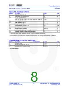
ABSOLUTE MAXIMUM RATINGS
Symbol
Parameter
Value
Unit
VCC
DC Supply Voltage at Pin 20
16
V
IOUT
Output Current at PG, Fb1, Fb2 Pins
V12, OP1, OP2, FB1, FB2, SS
30
mA
V
VPIN
-0.3 to 16
-0.3 to 7
1.5
PSON, V33, V5, VREF1, VREF2, OPP, UVAC, RI, NVP, IN, COMP, PG
Power Dissipation (TA=25°C)
V
PD,25℃
PD,90℃
TSTG
W
Power Dissipation (TA=90°C)
0.5
W
Storage Temperature Range
-55 to +150
82.5
°C
°C /W
°C
°C
°C
KV
Thermal Resistance, Junction-To-Air
Operating Junction Temperature
RθJA
TJ,MAX
TA,MAX
TL
150
Operating Ambient Temperature
-30 to +125
260
Lead Temperature (Soldering, 10 Seconds)
Electrostatic Discharge Capability, Human Body Model
ESD
3.0
*
*
All voltage values, except differential voltages, are given with respect to GND pin.
Stresses beyond those listed under "absolute maximum ratings" may cause permanent damage to the device.
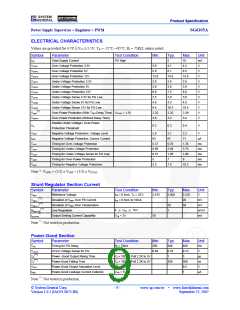
RECOMMENDED OPERATING CONDITIONS
Symbol
Parameter
Test Condition
Value
Unit
VCC
DC Supply Voltage
4.5 to 5.5
V
VFB
TA
Shunt Regulator Output Fb1, Fb2 Pins
Operating Ambient Temperature Range
4 to 16
V
-25 to +85
°C
* For proper operation.
© System General Corp.
Version 1.0.1 (IAO33.0072.B0)
- 8 -
www.sg.com.tw
•
www.fairchildsemi.com
September 25, 2007

 FAIRCHILD [ FAIRCHILD SEMICONDUCTOR ]