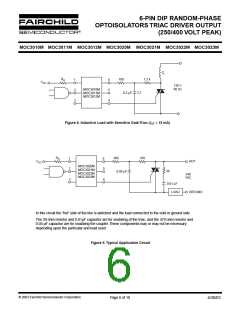
6-PIN DIP RANDOM-PHASE
OPTOISOLATORS TRIAC DRIVER OUTPUT
(250/400 VOLT PEAK)
MOC3010M MOC3011M MOC3012M MOC3020M MOC3021M MOC3022M MOC3023M
ELECTRICAL CHARACTERISTICS (T = 25°C Unless otherwise specified)
A
INDIVIDUAL COMPONENT CHARACTERISTICS
Parameters
Test Conditions
Symbol Device Min
Typ
Max Units
EMITTER
Input Forward Voltage
I = 10 mA
V
All
All
1.15
0.01
1.5
V
F
F
Reverse Leakage Current
DETECTOR
V = 3 V, T = 25°C
I
R
100
µA
R
A
Peak Blocking Current,Either Direction
Peak On-State Voltage,Either Direction
Rated V
, I = 0 (note 1)
I
DRM
All
All
10
100
3
nA
V
DRM
F
I
= 100 mA peak, I = 0
V
TM
1.8
TM
F
TRANSFER CHARACTERISTICS (T = 25°C Unless otherwise specified.)
A
DC Characteristics
Test Conditions
Symbol
Device
Min
Typ
Max
Units
MOC3020M
MOC3010M
MOC3021M
MOC3011M
MOC3022M
MOC3012M
MOC3023M
All
30
15
LED Trigger Current
Voltage = 3V (note 3)
I
mA
µA
FT
10
5
Holding Current, Either Direction
I
100
H
Note
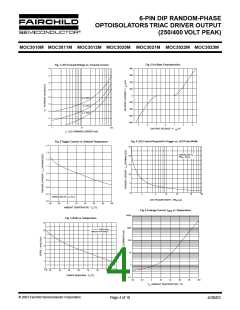
1. Test voltage must be applied within dv/dt rating.
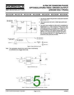
2. This is static dv/dt. See Figure 5 for test circuit. Commutating dv/dt is a function of the load-driving thyristor(s) only.
3. All devices are guaranteed to trigger at an I value less than or equal to max I . Therefore, recommended operating I lies
F
FT
F
between max I (30 mA for MOC3020M, 15 mA for MOC3010M and MOC3021M, 10 mA for MOC3011M and MOC3022M,
FT
5 mA for MOC3012M and MOC3023M) and absolute max I (60 mA).
F
© 2003 Fairchild Semiconductor Corporation
Page 3 of 10
4/30/03

 FAIRCHILD [ FAIRCHILD SEMICONDUCTOR ]