AC Electrical Characteristics
TA = −40 °C to +85 °C
CL = 50pF, RU = RD = 500Ω
Symbol
Parameter
Units
Conditions
Figure No.
V
CC = 4.5 – 5.5V CC = 4.0V
V
Min
Max
0.25
5.3
Min
Max
0.25
6.3
t
PHL,tPLH
tPZH, tPZL
tPHZ, tPLZ
Prop Delay Bus to Bus (Note 6)
Prop Delay, Select to Bus A
VI = OPEN
Figure 1
Figure 2
ns
ns
ns
1.0
1.0
1.0
1.0
1.0
Output Enable Time, Select to Bus B
Output Enable Time, IOE to Bus A, B
Output Disable Time., Select to Bus B
Output Disable Time, IOE to Bus A, B
5.3
6.0
VI = 7V for tPZL
Figure 1
Figure 2
5.3
6.2
VI = OPEN for tPZH
VI = 7V for tPLZ
5.8
6.2
Figure 1
Figure 2
5.5
6.2
VI = OPEN for tPHZ
Note 6: This parameter is guaranteed by design but is not tested. The bus switch contributes no propagation delay other than the RC delay of the typical On
resistance of the switch and the 50pF load capacitance, when driven by an ideal voltage the source (zero output impedance).
Capacitance (Note 7)
Symbol
Parameter
Typ
Max
Units
Conditions
VCC = 5.0V
CIN
CI/O
Control Pin Input Capacitance
3
13
5
pF
pF
pF
A Port
B Port
Input/Output Capacitance
VCC, OE = 5.0V
Note 7: TA = +25°C, f = 1 MHz, Capacitance is characterized but not tested.
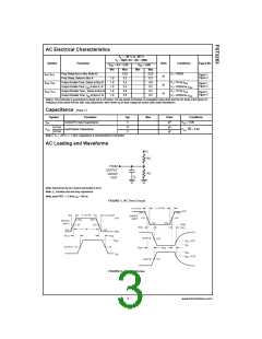
AC Loading and Waveforms
Note: Input driven by 50 Ω source terminated in 50 Ω
Note: CL includes load and stray capacitance
Note: Input PRR = 1.0 MHz, tW = 500 ns
FIGURE 1. AC Test Circuit
FIGURE 2. AC Waveforms
3
www.fairchildsemi.com

 FAIRCHILD [ FAIRCHILD SEMICONDUCTOR ]