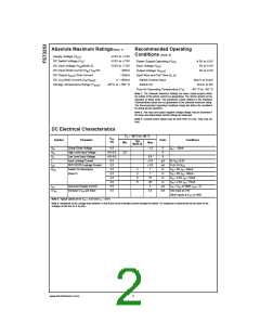
Absolute Maximum Ratings(Note 1)
Recommended Operating
Conditions (Note 3)
Supply Voltage (VCC
)
−0.5V to +7.0V
−0.5V to +7.0V
−0.5V to +7.0V
−50mA
DC Switch Voltage (VS)
Power Supply Operating (VCC)
4.0V to 5.5V
0V to 5.5V
0V to 5.5V
DC Input Voltage (VIN)(Note 2)
DC Input Diode Current (lIK) VIN<0V
DC Output (IOUT) Sink Current
Input Voltage (VIN
)
Output Voltage (VOUT
)
128mA
Input Rise and Fall Time (tr, tf)
Switch Control Input
DC VCC/GND Current (ICC/IGND
)
+/− 100mA
0ns/V to 5ns/V
0ns/V to DC
Storage Temperature Range (TSTG
)
−65°C to +150 °C
Switch I/O
Free Air Operating Temperature (TA)
−40 °C to −85 °C
Note 1: The Absolute Maximum Ratings are those values beyond which
the safety of the device cannot be guaranteed. The device should not be
operated at these limits. The parametric values defined in the Electrical
Characteristics tables are not guaranteed at the absolute maximum rating.
The Recommended Operating Conditions tables will define the conditions
for actual device operation.
Note 2: The input and output negative voltage ratings may be exceeded if
the input and output diode current ratings are observed.
Note 3: Unused control inputs must be held HIGH or LOW. They may not
float.
DC Electrical Characteristics
T
A = −40 °C to +85 °C
VCC
(V)
Symbol
Parameter
Units
Conditions
Typ
Min
Max
(Note 4)
VIK
Clamp Diode Voltage
High Level Input Voltage
Low Level Input Voltage
Input Leakage Current
OFF-STATE Leakage Current
Switch On Resistance
(Note 5)
4.5
4.0–5.5
4.0–5.5
5.5
−1.2
V
V
IIN = −18mA
VIH
VIL
II
2.0
0.8
±1.0
±1.0
7
V
µA
µA
Ω
0≤ VIN ≤5.5V
0 ≤A, B ≤VCC
IOZ
RON
5.5
4.5
4
4
V
V
V
V
V
IN = 0V, IIN = 64mA
4.5
7
Ω
IN = 0V, IIN = 30mA
4.5
8
15
20
3
Ω
IN = 2.4V, IIN = 15mA
IN = 2.4V, IIN = 15mA
IN = VCC or GND, IOUT = 0
4.0
11
Ω
ICC
Quiescent Supply Current
Increase in ICC per Input
5.5
µA
mA
∆ ICC
5.5
2.5
One input at 3.4V
Other inputs at VCC or GND
Note 4: Typical values are at VCC = 5.0V and TA = +25°C
Note 5: Measured by the voltage drop between A and B pins at the indicated current through the switch. On resistance is determined by the lower of the
voltages on the two (A or B) pins.
www.fairchildsemi.com
2

 FAIRCHILD [ FAIRCHILD SEMICONDUCTOR ]