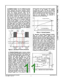
4.3. Output-Short Protection (OSP): If the output is
shorted, steep current with extremely high di/dt can
flow through the SenseFET during the minimum turn-
on time. Such a steep current creates high-voltage
stress on the drain of the SenseFET when turned off.
To protect the device from this abnormal condition,
OSP is included. It is comprised of detecting VFB and
SenseFET turn-on time. When the VFB is higher than
2.0V and the SenseFET turn-on time is lower than
1.0μs, the FSL117MRIN recognizes this condition as
an abnormal error and shuts down PWM switching
until VCC reaches VSTART again. An abnormal condition
output short is shown in Figure 23.
4.6 Line Over-Voltage Protection (LOVP): If the line
input voltage is increased until unwanted level, high
line input voltage brings high-voltage stress on the
entire system. To protect from this abnormal
condition, LOVP is included. It is comprised of
detecting VIN using divided resistors. When VIN is
higher than 1.95V, this condition is recognized as an
abnormal error and PWM switching shuts down until
VIN decreases to around 1.89V (60mV hysteresis).
Figure 24. Line Over-Voltage Protection
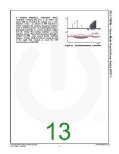
5. Soft Burst Mode: To minimize power dissipation in
Standby Mode, the FSL117MRIN enters Burst Mode.
As the load decreases, the feedback voltage
decreases. The device automatically enters Burst
Mode when the feedback voltage drops below VBURL
(300mV), as shown in Figure 25. At this point,
switching stops and the output voltages start to drop
at a rate dependent on standby current load. This
causes the feedback voltage to rise. Once it passes
VBURH (450mV), switching resumes. Feedback voltage
then falls and the process repeats. Burst Mode
alternately enables and disables switching of the
SenseFET, reducing switching loss in Standby Mode.
Figure 23. Output-Short Protection
4.4 Over-Voltage Protection (OVP): If the
secondary-side feedback circuit malfunctions or a
solder defect causes an opening in the feedback path,
the current through the opto-coupler transistor
becomes almost zero. Then VFB climbs up in a similar
manner to the overload situation, forcing the preset
maximum current to be supplied to the SMPS until the
overload protection is triggered. Because more
energy than required is provided to the output, the
output voltage may exceed the rated voltage before
the overload protection is triggered, resulting in the
breakdown of the devices in the secondary side. To
prevent this situation, an OVP circuit is employed. In
general, the VCC is proportional to the output voltage
and the FSL117MRIN uses VCC instead of directly
monitoring the output voltage. If VCC exceeds 24.5V,
an OVP circuit is triggered, resulting in the termination
of the switching operation. To avoid undesired
activation of OVP during normal operation, VCC should
be designed to be below 24.5V.
4.5 Thermal Shutdown (TSD): The SenseFET and
the control IC on a die in one package makes it easier
for the control IC to detect the temperature of the
SenseFET. If the temperature exceeds ~140C, the
thermal shutdown is triggered and stops operation.
The FSL117MRIN operates in auto-restart mode until
the temperature decreases to around 75C, when
normal operation resumes.
Figure 25. Burst-Mode Operation
© 2012 Fairchild Semiconductor Corporation
FSL117MRN • Rev.1.0.0
www.fairchildsemi.com
12

 FAIRCHILD [ FAIRCHILD SEMICONDUCTOR ]