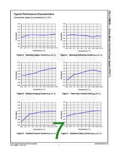
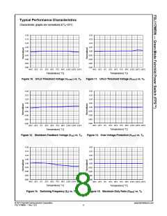
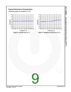
Functional Description
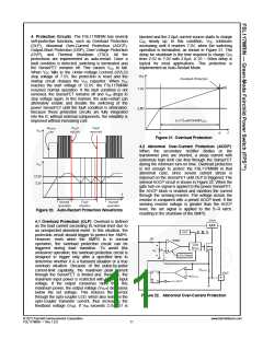
1. Startup: At startup, an internal high-voltage current
source supplies the internal bias and charges the
external capacitor (CVcc) connected to the VCC pin, as
illustrated in Figure 18. When VCC reaches 12V, the
FSL117MRIN begins switching and the internal high-
voltage current source is disabled. Normal switching
operation continues and the power is supplied from the
auxiliary transformer winding unless VCC goes below the
stop voltage of 7.5V.
3. Feedback Control: This device employs current-
mode control, as shown in Figure 19. An opto-coupler
(such as the FOD817) and shunt regulator (such as the
KA431) are typically used to implement the feedback
network. Comparing the feedback voltage with the
voltage across the RSENSE resistor makes it possible to
control the switching duty cycle. When the reference pin
voltage of the shunt regulator exceeds the internal
reference voltage of 2.5V, the opto-coupler LED current
increases, pulling down the feedback voltage and
reducing drain current. This typically occurs when the
input voltage is increased or the output load is decreased.
3.1 Pulse-by-Pulse Current Limit: Because current-
mode control is employed, the peak current through
the SenseFET is limited by the inverting input of the
PWM comparator (VFB*), as shown in Figure 19.
Assuming that the 90μA current source flows only
through the internal resistor (3R + R = 27kꢀ), the
cathode voltage of diode D2 is about 2.5V. Since D1
is blocked when the feedback voltage (VFB) exceeds
2.5V, the maximum voltage of the cathode of D2 is
clamped at this voltage. Therefore, the peak value of
the current through the SenseFET is limited.
3.2 Leading-Edge Blanking (LEB): At the instant the
internal SenseFET is turned on, a high-current spike
usually occurs through the SenseFET, caused by
primary-side capacitance and secondary-side rectifier
reverse recovery. Excessive voltage across the RSENSE
resistor leads to incorrect feedback operation in the
current-mode PWM control. To counter this effect, the
FSL117MRIN employs a leading-edge blanking (LEB)
circuit. This circuit inhibits the PWM comparator for
tLEB (300ns) after the SenseFET is turned on.
Figure 18. Startup Block
2. Soft-Start: The internal soft-start circuit increases the
PWM comparator inverting input voltage, together with
the SenseFET current, slowly after startup. The typical
soft-start time is 15ms. The pulse width to the power
switching device is progressively increased to establish
the correct working conditions for transformers,
inductors, and capacitors. The voltage on the output
capacitors is progressively increased to smoothly
establish the required output voltage. This helps prevent
transformer saturation and reduces stress on the
secondary diode during startup.
Figure 19. Pulse Width Modulation Circuit
© 2012 Fairchild Semiconductor Corporation
FSL117MRN • Rev.1.0.0
www.fairchildsemi.com
10

 FAIRCHILD [ FAIRCHILD SEMICONDUCTOR ]