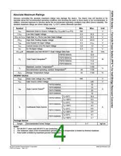
Absolute Maximum Ratings
Stresses exceeding the absolute maximum ratings may damage the device. The device may not function or be
operable above the recommended operating conditions and stressing the parts to these levels is not recommended. In
addition, extended exposure to stresses above the recommended operating conditions may affect device reliability. The
absolute maximum ratings are stress ratings only. TA=25°C unless otherwise specified.
Symbol
VDS
Parameter
Maximum Drain-to-Source Voltage (VDL-VCTR and VCTR-PG)
Low-Side Supply Voltage
Min.
500
-0.3
-0.3
-0.3
-0.3
-5.0
-0.3
Max.
Unit
V
LVCC
25.0
25.0
525.0
LVCC
1.0
V
HVCC to VCTR High-Side VCC Pin to Low-Side Drain Voltage
V
HVCC
VAR
High-Side Floating Supply Voltage
Auto-Restart Pin Input Voltage
Current-Sense (CS) Pin Input Voltage
RT Pin Input Voltage
V
V
VCS
V
VRT
5.0
V
dVCTR/dt
Allowable Low-Side MOSFET Drain Voltage Slew Rate
FSFR2100XS/L
50
V/ns
12.0
11.7
11.6
11.5
+150
+130
+150
FSFR1800XS/L
PD
Total Power Dissipation(3)
W
FSFR1700XS/L
FSFR1600XS/L
Maximum Junction Temperature(4)
Recommended Operating Junction Temperature(4)
Storage Temperature Range
TJ
°C
°C
-40
-55
TSTG
MOSFET Section
VDGR
VGS
500
V
V
Drain Gate Voltage (RGS=1MΩ)
Gate Source (GND) Voltage
±30
32
FSFR2100XS/L
FSFR1800XS/L
FSFR1700XS/L
FSFR1600XS/L
23
IDM
Drain Current Pulsed(5)
A
20
18
10.5
6.5
7.0
4.5
6.0
3.9
4.5
2.7
TC=25°C
TC=100°C
TC=25°C
TC=100°C
TC=25°C
TC=100°C
TC=25°C
TC=100°C
FSFR2100XS/L
FSFR1800XS/L
FSFR1700XS/L
FSFR1600XS/L
ID
Continuous Drain Current
A
Package Section
Torque Recommended Screw Torque
Notes:
3. Per MOSFET when both MOSFETs are conducting.
5~7
kgf·cm
4. The maximum value of the recommended operating junction temperature is limited by thermal shutdown.
5. Pulse width is limited by maximum junction temperature.
© 2010 Fairchild Semiconductor Corporation
FSFR-XS Series • Rev.1.0.1
www.fairchildsemi.com
4

 FAIRCHILD [ FAIRCHILD SEMICONDUCTOR ]