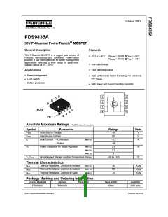
Typical Characteristics
10
800
700
600
500
400
300
200
100
0
ID = -5.3A
f = 1 MHz
VGS = 0 V
VDS = -5V
-10V
8
6
4
2
0
-15V
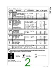
CISS
COSS
CRSS
0
2
4
6
8
10
0
5
10
15
20
25
30
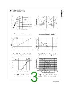
Qg, GATE CHARGE (nC)
-V DS, DRAIN TO SOURCE VOLTAGE (V)
Figure 7. Gate Charge Characteristics.
Figure 8. Capacitance Characteristics.
100
10
50
40
30
20
10
0
SINGLE PULSE
100
s
m
Rq = 125°C/W
JA
RDS(ON) LIMIT
1ms
10ms
100ms
1s
TA = 25°C
1
10s
DC
VGS = -10V
SINGLE PULSE
RqJA = 125oC/W
TA = 25oC
0.1
0.01
0.1
1
10
100
0.001
0.01
0.1
1
10
100
1000
-VDS , DRAIN-SOURCE VOLTAGE (V)
t1, TIME (sec)
Figure 9. Maximum Safe Operating Area.
Figure 10. Single Pulse Maximum
Power Dissipation.
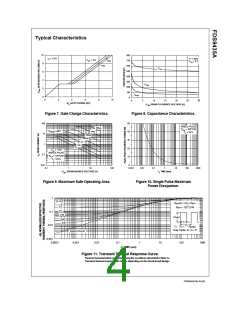
1
D = 0.5
RqJA(t) = r(t) + RqJA
RqJA = 125oC/W
0.2
0.1
0.1
0.05
0.02
P(pk)
t1
0.01
t2
0.01
TJ - TA = P * R JA(t)
q
Duty Cycle, D = t1 / t2
SINGLE PULSE
0.001
0.0001
0.001
0.01
0.1
1
10
100
1000
t1, TIME (sec)
Figure 11. Transient Thermal Response Curve.
Thermal characterization performed using the conditions described in Note 1c.
Transient thermal response will change depending on the circuit board design.
FDS9435A Rev D1(W)

 FAIRCHILD [ FAIRCHILD SEMICONDUCTOR ]