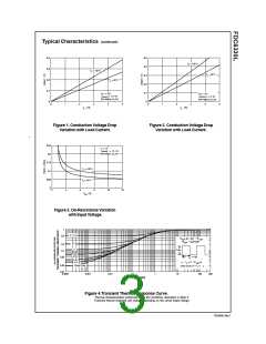
Typical Characteristics (continued)
0.4
0.3
0.5
0.4
0.3
0.2
0.1
0
T
= 125°C
J
T
= 125°C
J
T
= 25°C
J
0.2
0.1
0
T = 25°C
J
V
V
= 12V
V
V
= 5V
IN
IN
= 1. 5- 8 V
= 1. 5- 8 V
ON/OF F
ON/OF F
PW =300us, D 2%
PW =300us, D 2%
≤
≤
0
1
2
3
4
5
0
1
2
3
4
5
I
, (A)
I , (A)
L
L
Figure 1. Conduction Voltage Drop
Variation with Load Current.
Figure 2. Conduction Voltage Drop
Variation with Load Current.
0.25
0.2
I
= 1 A
L
V
= 1.5 - 8 V
ON/OFF
PW =300us, D 2%
≤
0.15
0.1
T
= 125°C
J
0.05
0
T
=
25°C
, ( V)
J
2
4
6
8
10
12
V
IN
Figure 3. On-Resistance Variation
with Input Voltage.
1
D = 0.5
0.5
R
(t) = r(t) * R
JA
θ
JA
θ
R
=180°C/W
JA
θ
0.2
0.2
0.1
P(pk)
0.1
0.05
t
1
0.05
t
2
0.02
0.01
T
- T = P * R
(t)
JA
J
A
θ
Single Pulse
0.02
Duty Cycle, D = t / t
2
1
0.01
0.0001
0.001
0.01
0.1
t1, TIME (sec)
1
10
100
300
Figure 4.Transient Thermal Response Curve.
Thermal characterization performed using the conditions described in Note 2.
Transient themal response will change depending on the circuit board design.
FDC6330L Rev. C

 FAIRCHILD [ FAIRCHILD SEMICONDUCTOR ]