TA=25oC unless otherwise noted
Electrical Characteristics
Symbol
Parameter
Test Conditions
Min Typ Max Units
OFF Characteristics
IFL
Leakage Current
VIN = 20 V, VON/OFF = 250
A
1
A
µ
µ
(Note 3)
ON Characteristics
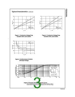
VDROP
Conduction Voltage
VIN = 12 V, VON/OFF = 3.3 V, IL = 2.5 A
VIN = 5 V, VON/OFF = 3.3 V, IL = 1.6 A
0.2
0.2
V
V
R(ON)
IL
Q2 - Static On-Resistance VGS = -12 V, ID = -2.3 A
GS = -5 V, ID = -1.9 A
0.054
0.081
0.08
0.125
Ω
V
Load Current
VDROP = 0.2 V, VIN = 12 V, VON/OFF = 3.3 V
2.5
1.6
A
VDROP = 0.2 V, VIN = 5 V, VON/OFF = 3.3 V
Notes:
1. Range of V can be up to 30V, but R and R must be scaled such that V
of Q2 does not exceed 20V.
is the sum of the junction-to-case and case-to-ambient thermal resistance where the case thermal reference is defined as the solder mounting
i
n
1
2
G
S
2. R
θJA
surface of the drain pins. R
is guaranteed by design while R
is determined by the user’s board design.
θJC
θJA
3. Pulse Test: Pulse Width < 300µs, Duty Cycle < 2.0%.
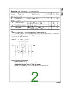
FDC6330L Load Switch Application
External Component Recommendation:
For applications where Co ≤ 1µF.
For slew rate control, select R2 in the range of 1k - 4.7kΩ .
For additional in-rush current control,C1 ≤ 1000pF can be added.
Select R1 so that the R1/R2 ratio ranges from 10 - 100. R1 is required to turn Q2 off.
FDC6330L Rev. C

 FAIRCHILD [ FAIRCHILD SEMICONDUCTOR ]