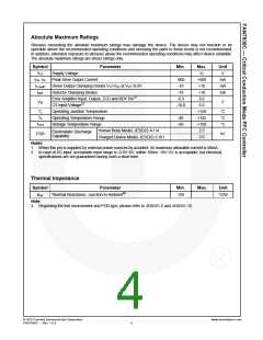
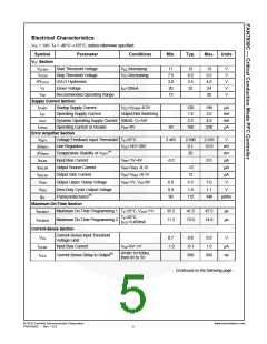
Absolute Maximum Ratings
Stresses exceeding the absolute maximum ratings may damage the device. The device may not function or be
operable above the recommended operating conditions and stressing the parts to these levels is not recommended.
In addition, extended exposure to stresses above the recommended operating conditions may affect device reliability.
The absolute maximum ratings are stress ratings only.
Symbol
VCC
Parameter
Min.
Max.
VZ
Unit
V
Supply Voltage
IOH, IOL
ICLAMP
IDET
Peak Drive Output Current
-800
-10
+500
+10
+10
8.0
mA
mA
mA
Driver Output Clamping Diodes VO>VCC or VO<-0.3V
Detector Clamping Diodes
-10
Error Amplifier Input, Output, ZCD and RDY Pin(1)
CS Input Voltage(2)
-0.3
-10.0
VIN
V
6.0
TJ
TA
Operating Junction Temperature
Operating Temperature Range
+150
+125
+150
2.5
°C
°C
°C
-40
-65
TSTG
Storage Temperature Range
Human Body Model, JESD22-A114
Charged Device Model, JESD22-C101
Electrostatic Discharge
Capability
ESD
kV
2.0
Notes:
1. When this pin is supplied by external power sources by accident, its maximum allowable current is 50mA.
2. In case of DC input, acceptable input range is -0.3V~6V: within 100ns -10V~6V is acceptable, but electrical
specifications are not guaranteed during such a short time.
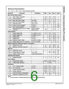
Thermal Impedance
Symbol
Parameter
Min.
Max.
Unit
Thermal Resistance, Junction-to-Ambient(3)
150
°C/W
ΘJA
Note:
3. Regarding the test environment and PCB type, please refer to JESD51-2 and JESD51-10.
© 2010 Fairchild Semiconductor Corporation
www.fairchildsemi.com
FAN7930C • Rev. 1.0.0
4

 FAIRCHILD [ FAIRCHILD SEMICONDUCTOR ]