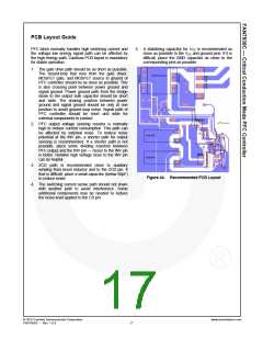
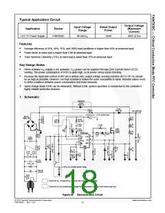
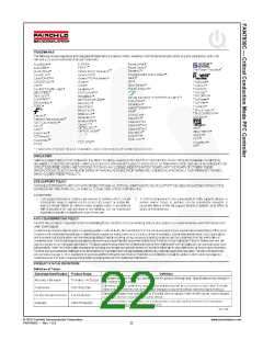
Typical Application Circuit
Output Voltage
(Maximum
Current)
Input Voltage
Range
Rated Output
Power
Application
Device
FAN7930C
LCD TV Power Supply
90-265VAC
195W
390V (0.5A)
Features
Average efficiency of 25%, 50%, 75%, and 100% load conditions is higher than 95% at universal input.
Power factor at rated load is higher than 0.98 at universal input.
Total Harmonic Distortion (THD) at rated load is lower than 15% at universal input.
Key Design Notes
When auxiliary VCC supply is not available, VCC power can be supplied through Zero Current Detect (ZCD)
winding. The power consumption of R103 is quite high, so its power rating needs checking.
Because the input bias current of INV pin is almost zero, output voltage sensing resistors (R112~R115) should
be as high as possible. However, too-high resistance makes the node susceptible to noise. Resistor values need
to strike a balance between power consumption and noise immunity.
Quick-charge diode D106 can be eliminated. Without D106, system operation is normal due to the controller’s
highly reliable protection features.
1. Schematic
Optional
D106
600V 3A
D105
600V 8A
230mH,
49:6
DC OUTPUT
LP101,EER3124N
BD101,
600V,15A
VAUX
R103,
10k,1W
C104,
12nF
R109
47
Q101
FCPF
20N60
D102,
UF4004
FAN7930C
D103,1N414
8
R108
4.7
8
7
VCC
ZC
Out
C102,
680nF
5
3
2
4
1
D
CS
Com
p
INV
RD
Y
GND
6
C114 C115
,2.2n ,2.2n
F
F
C101,
220nF
R101,1M-
J
VCC for another power stage
ZNR101
,10D471
Circuit for VCC. If external VCC is used, this circuit is not needed.
Circuit for VCC for another power stage thus components structure and values may vary.
Figure 45. Demonstration Circuit
© 2010 Fairchild Semiconductor Corporation
FAN7930C • Rev. 1.0.0
www.fairchildsemi.com
18

 FAIRCHILD [ FAIRCHILD SEMICONDUCTOR ]