PRODUCT SPECIFICATION
FAN5066
Absolute Maximum Ratings
Supply Voltages, VCCA, VCCP, VCCQP to GND
13V
18V
Supply Voltage VCCQP, Charge Pump (V +VCCA)
IN
Voltage Identification Code Inputs, VID3-VID0
VREF Output Current
13V
3mA
150°C
Junction Temperature, T
Storage Temperature
J
-65 to 150°C
300°C
Lead Soldering Temperature, 10 seconds
Operating Conditions
Parameter
Conditions
Min.
Typ.
Max.
Units
Supply Voltage, VCCA, VCCP
4.75
5
5.25
V
V
Input Logic HIGH
2.0
Input Logic LOW
0.8
70
12
V
Ambient Operating Temp
Output Driver Supply, VCCQP
0
°C
V
8.5
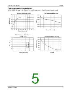
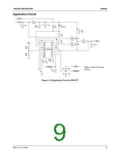
Electrical Specifications
(V
CCA
= 5V, V
= 900mV, f
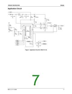
= 300 KHz, and T = +25°C using circuit in Figure 1, unless otherwise noted)
osc A
CNTRL
The • denotes specifications which apply over the full operating temperature range.
Parameter
Conditions
Min.
Typ.
Max. Units
Initial Voltage Setpoint
I
= 0.8A, V
V
= 1.25V
= 900mV
1.237 1.250 1.263
V
mV
LOAD
CTRL
CTRL
891
900
909
Output Temperature Drift
T = 0 to 70°C V
= 1.25V
= 900mV
•
•
+6
+4
mV
mV
A
OUT
OUT
V
Load Regulation
I
= 0.8A to 3A
•
•
-20
±2
mV
mV
mVpk
V
LOAD
Line Regulation
V
= 4.75V to 5.25V
IN
Output Ripple
20MHz BW, I
= 3A
±13
LOAD
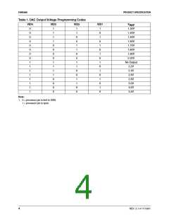
DAC Output Voltage
DAC Accuracy
See Table 1
1.3
-3
3.4
+3
%
Short Circuit Detect Threshold
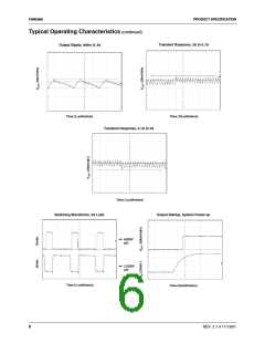
Output Driver Rise and Fall Time
Output Driver Deadtime 1
Output Driver Deadtime 2
Turn-on Response Time
Oscillator Range
•
90
120
80
5
150
mV
nsec
See Figure 3
See Figure 3
See Figure 3
%/f
OSC
80
nsec
I
= 0A to 3A
10
msec
KHz
KHz
LOAD
80
1000
330
Oscillator Frequency
PWRGD threshold
C
EXT
= 100 pF
270
300
Logic High
Logic Low
93
88
107 %V
112 %V
OUT
OUT
PWRGD Minimum Operating
Voltage
1.0
95
V
Max Duty Cycle
90
%
Control Pin Input Current
V
CTRL
= 400mV to 3.5V
•
235
µA
REV. 2.1.4 11/13/01
3

 FAIRCHILD [ FAIRCHILD SEMICONDUCTOR ]