FAN5066
PRODUCT SPECIFICATION
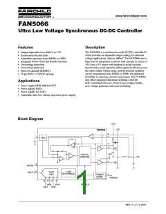
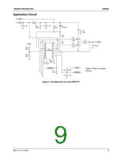
Pin Assignments
CEXT
ENABLE
PWRGD
IFB
1
2
20
19
18
17
16
15
14
13
12
11
VREF
VID1
3
VID2
4
VID3
VFB
5
CNTRL
GNDA
GNDD
VCCQP
HIDRV
GNDP
FAN5066
VCCA
VCCP
VID4
6
7
8
LODRV
GNDP
9
10
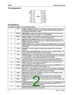
Pin Definitions
Pin Number Pin Name Pin Function Description
1
CEXT
Oscillator Capacitor Connection. Connecting an external capacitor to this pin sets
the internal oscillator frequency. Layout of this pin is critical to system performance.
See Application Information for details.
2
3
4
ENABLE Output Enable. A logic LOW on this pin will disable the output. An internal pull-up
resistor allows for either open collector or TTL compatibility.
PWRGD Power Good Flag. An open collector output that will be at logic LOW if the output
voltage is not within ±12% of the nominal output voltage setpoint.
IFB
High Side Current Feedback. Pins 4 and 5 are used as the inputs for the current
feedback control loop. Layout of these traces is critical to system performance. See
Application Information for details.
5
VFB
Voltage Feedback. Pin 5 is used as the input for the voltage feedback control loop and
as the low side current feedback input. See Application Information for details regarding
correct layout.
6
7
8
VCCA
VCCP
VID4
Analog VCC. Connect to system 5V supply and decouple with a 0.1µF ceramic
capacitor.
Power VCC for low side FET driver. Connect to system 5V supply and place a 1µF
ceramic capacitor for decoupling and local charge storage.
VID4 Input. A logic 1 on this open collector/TTL input will enable the VID3–VID0 inputs
to set the output from 2.1V to 3.5V, and a logic 0 will set the output from 1.3V to 2.05V,
as shown in Table 1. Pullup resistors are internal to the controller.
9
10, 11
12
LODRV
GNDP
Low Side FET Driver. Connect this pin to the gate of an N-channel MOSFET for
synchronous operation. The trace from this pin to the MOSFET gate should be < 0.5".
Power Ground. Return pin for high currents flowing in pins 7 and 13 (VCCP and
VCCQP). Connect to a low impedance ground.
HIDRV
VCCQP
High Side FET Driver. Connect this pin to the gate of an N-channel MOSFET. The
trace from this pin to the MOSFET gate should be < 0.5".
13
Power VCC. For high side FET driver. VCCQP must be connected to a voltage of at
least VCCA + V
(MOSFET), and place a 1µF ceramic capacitor for decoupling
GS,ON
and local charge storage. See Application Information for details
14
15
GNDD
GNDA
CNTRL
Digital Ground. Return path for digital logic. Connect to a low impedance system
ground plane to minimize ground loops.
Analog Ground. Return path for low power analog circuitry. This pin should be
connected to a low impedance system ground plane to minimize ground loops.
16
Voltage Control. The voltage forced on this pin determines the output voltage of the
converter.
17-19
VID1-VID3 Voltage Identification Code Inputs. These open collector/TTL compatible inputs will
program the output voltage of the reference over the ranges specified in Table 1.
Pull-up resistors are internal to the controller.
20
VREF
Reference Voltage Test Point. This pin provides access to the DAC output and should
be decoupled to ground using 0.1µF capacitor.
2
REV. 2.1.4 11/13/01

 FAIRCHILD [ FAIRCHILD SEMICONDUCTOR ]