AN-8019
APPLICATION NOTE
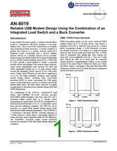
In concert with the FPF2195 for OCP, the FAN8060, a 1A
synchronous step-down converter, manages 2A pulsed load
applications. Its 1.2MHz fixed switching frequency allows
for a low profile inductor, which is ideal for compact power-
management applications. The user-defined external
compensation provides a more flexible design to meet
dynamic characteristics with large bulk capacitors required
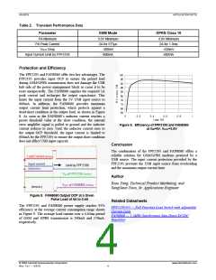
by most pulsed-load conditions. With the soft-start pin, the
startup time can be adjusted without a large inrush to charge
the reservoir capacitors. Figure 5 shows a waveform of
charging the output capacitors. While the VOUT rising time is
23ms, a 82nF capacitor is used to turn the system on slowly.
The FAN8060’s SYNC pin can be used for both maximum
load current limit function and to improve EMI
characteristics. When the SYNC pin is connected to the VIN
and GND, the peak inductor current is limited to 0.6A and
1.2A, respectively. In addition, when applying an external
PWM signal to the SYNC pin, the internal oscillator is
synchronized to improve EMI characteristics.
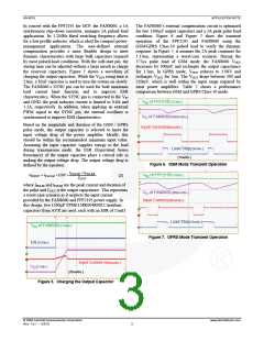
The FAN8060’s external compensation circuit is optimized
for two 1500µF output capacitors and a 2A peak pulse load
condition. Figure 6 and Figure 7 show the transient
operation of the FPF2195 and FAN8060 using the
GSM/GPRS Class-10 pulsed load to verify the dynamic
response. In Figure 7, it assumes the 2A peak continues for
1.15ms, representing a worst-case scenario. During the
577µs pulse load of GSM mode, the FAN8060 VOUT
decreases by 300mV and recharges the output capacitance
for 1.5ms. In GPRS mode, VOUT reduces to 3.08V and
recharges VOUT for 2ms. The VOUT drops between 300 and
520mV, which is well within the input range required by
most power amplifiers. Table 2 shows a performance
comparison between GSM and GPRS Class-10 mode.
Vin of FPF2195 [1V/div.]
V
of FPF2195 [1V/div.]
IN
O
Vo of FAN8060 [500mV/div.]
of FAN8060[500mV/div.]
V
Based on the magnitude and duration of the GSM / GPRS
pulse mode, the output capacitor is selected to meet the
input voltage drop of the power amplifier. Ideally, this
should be within the recommended minimum input value.
Assuming the input capacitor supplies energy to the load
during transmission mode, the ESR (Equivalent Series
Resistance) of the output capacitor plays a critical role in
making the output voltage drop. The output voltage drop is
defined by the equation:
Input Current[500mA/div.]
Inpu current [500mA/div.]
Load Step[2A/vdiv.]
Load step [2A/vdiv.]
[1ms/div.]
[1ms/div.]
Figure 6. GSM Mode Transient Operation
I
× t
PULSE
PULSE
V
= I
× ESR +
PULSE
V
V
of FPF2195 [1V/div.]
(2)
DROP
IN
O
C
OUT
where IPULSE and tPULSE are the peak current and duration of
the pulse and COUT is the output capacitance. This represents
a worst-case scenario as it neglects the input current
of FAN8060 [500mV/div.]
provided by the FAN8060 and FPF2195 power supply. In
this design, two 1500µF TPME158K004R0015 tantalum
capacitors from AVX are used, each with an ESR of 15mΩ.
Input Current[500mA/div.]
Load Step[2A/vdiv.]
V
of FAN8060 [1V/div.]
IN
Figure 7. GPRS Mode Transient Operation
EN [2V/div.]
Input Current [500mA/div.]
V
[1V/div.]
O
[20ms/div.]
Figure 5. Charging the Output Capacitor
© 2009 Fairchild Semiconductor Corporation
Rev. 1.0.1 • 5/3/10
www.fairchildsemi.com
3

 FAIRCHILD [ FAIRCHILD SEMICONDUCTOR ]